Piezoelectric film bulk acoustic wave resonator and preparation method thereof
A technology of bulk acoustic wave resonator and piezoelectric film, applied in electrical components, impedance networks, etc., can solve problems such as poor thermal conductivity, and achieve the effects of improving mechanical strength, reducing process steps, and reducing process difficulty
- Summary
- Abstract
- Description
- Claims
- Application Information
AI Technical Summary
Problems solved by technology
Method used
Image
Examples
Embodiment 1
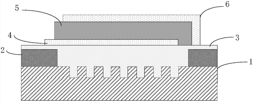
[0043] This embodiment provides a piezoelectric film bulk acoustic resonator, the structure of which is as follows figure 1 As shown, it includes a substrate 1 provided with vertical grooves, a patterned support layer 2, a low acoustic impedance layer 3 completely filling the surface of the substrate, a bottom electrode layer 4, a piezoelectric layer 5, and a top electrode layer 6; In this embodiment, the substrate material is silicon, the depth of the vertical grooves in the substrate is about 10um, the vertical grooves are square holes, the vertical grooves are arranged in an array, and the shape of the side view is a comb line. The low acoustic impedance layer is polyimide, the bottom electrode is molybdenum, the piezoelectric layer is aluminum nitride with C-axis orientation, and the uppermost top electrode is metal molybdenum.
[0044] The specific preparation process of the piezoelectric thin film bulk acoustic resonator includes the following steps:
[0045]Step 1. Us...
PUM
 Abstract
Description
Claims
Application Information
 - R&D
- Intellectual Property
- Life Sciences
- Materials
- Tech Scout
- Unparalleled Data Quality
- Higher Quality Content
- 60% Fewer Hallucinations
Browse by: Latest US Patents, China's latest patents, Technical Efficacy Thesaurus, Application Domain, Technology Topic, Popular Technical Reports.
© 2025 PatSnap. All rights reserved.Legal|Privacy policy|Modern Slavery Act Transparency Statement|Sitemap|About US| Contact US: help@patsnap.com


