Manufacturing and application of semiconductor nanometer ultraviolet light detection and gas sensing integrating device

A gas sensing and integrated device technology, applied in semiconductor devices, electrical components, instruments, etc., can solve problems affecting the working stability of semiconductor nano-ultraviolet photodetection devices, achieve simple structure, high sensitivity, and solve unstable performance problems. Effect

Inactive Publication Date: 2017-08-25
UNIV OF SHANGHAI FOR SCI & TECH
View PDF5 Cites 3 Cited by
  • Summary
  • Abstract
  • Description
  • Claims
  • Application Information

AI Technical Summary

Problems solved by technology

[0003] The invention aims at the problem that the environment will affect the working stability of semiconductor nano-ultraviolet light detection devices, and proposes the manufacture and application of a semiconductor nano-ultraviolet light detection and gas sensing integrated device, which is made of two-dimensional structure semiconductor nanomaterials. It can not only stably detect ultraviolet light signals under different ambient atmosphere conditions, but also detect different organic gas molecules at room temperature

Method used


Image

  • Manufacturing and application of semiconductor nanometer ultraviolet light detection and gas sensing integrating device
  • Manufacturing and application of semiconductor nanometer ultraviolet light detection and gas sensing integrating device
  • Manufacturing and application of semiconductor nanometer ultraviolet light detection and gas sensing integrating device

Examples


Embodiment Construction

[0024] The semiconductor nano-ultraviolet light detection and gas sensing integrated device utilizes the characteristics of two-dimensional semiconductor nano-materials with large specific surface area and sensitivity to organic gas molecules, without any other complicated process and special structural design, to achieve Stable detection of ultraviolet light signals and detection of organic molecules at room temperature.

[0025] The manufacture and test application of a semiconductor nano-ultraviolet light detection and gas sensing integrated device, the specific implementation steps are as follows:

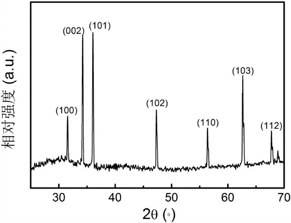
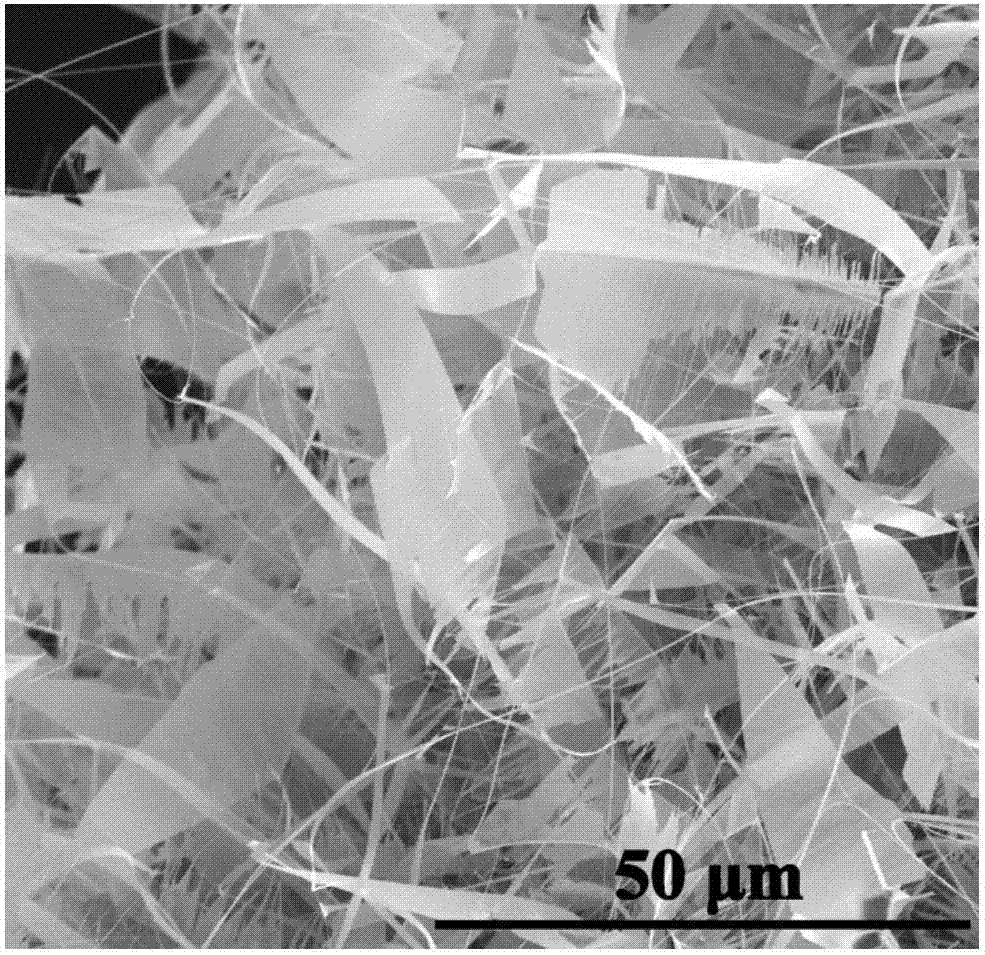
[0026] (1) Using chemical vapor deposition method, in p-type Si / SiO 2 Synthesize the two-dimensional structure ZnO semiconductor nanosheets in the middle section of the insulating substrate surface; p-type Si / SiO 2 The length of the insulating substrate is 1mm~20mm, the width is 1mm~20mm, the p-type Si substrate is a single crystal or polycrystalline structure, SiO 2 Layer th...


PUM

PropertyMeasurementUnit
Thicknessaaaaaaaaaa
Lengthaaaaaaaaaa
Widthaaaaaaaaaa

Abstract

The invention relates to manufacturing and application of a semiconductor nanometer ultraviolet light detection and gas sensing integrating device. A chemical vapor deposition method is adopted, in the middle section of the surface of a p-type Si / SiO2 substrate, a two-dimensional structure ZnO semiconductor nanosheet is compounded, symmetrical Au / Ti metal electrodes are plated along the two ends of the compounded ZnO nanosheet, any one of polymers in PDMS, PMMA and PVC is adopted to coat a metal electrode layer, and aluminum foil non-transparent to ultraviolet and visible light is utilized to block out other parts except the middle two-dimensional structure ZnO semiconductor nanosheet to prepare into the device. According to the manufacturing and application of the semiconductor nanometer ultraviolet light detection and gas sensing integrating device, the purposes of stably probing ultraviolet signals under different environment atmosphere conditions and detecting organism molecules under room temperature conditions are achieved, and the problem that a semiconductor ultraviolet detector is instable in performance under environment atmosphere conditions is solved. The semiconductor nanometer ultraviolet light detection and gas sensing integrating device has the advantages of being simple in structure, fast in response, high in sensitivity and capable of working under room temperature.

Description

technical field [0001] The invention relates to a semiconductor technology, in particular to the manufacture and application of a semiconductor nanometer ultraviolet light detection and gas sensing integrated device. Background technique [0002] Semiconductor ultraviolet light detectors have the advantages of fast response, good selectivity, high response rate, and high signal-to-noise ratio, and are widely used in security communication, chemical analysis, and environmental monitoring. Most of the common semiconductor ultraviolet photodetectors are based on the photoconductive effect of wide bandgap semiconductors. Using ultraviolet light to irradiate semiconductors makes electrons in the valence band transition to the conduction band to form non-equilibrium carriers, which significantly increases the conductivity of semiconductor materials and realizes ultraviolet light detection. Detection of optical signals. The rapid development of various intelligent and integrated m...

Claims


Application Information

Patent Timeline
IPC IPC(8): G01N27/48G01R27/02H01L31/18
CPCG01N27/48G01R27/02H01L31/18Y02P70/50
Inventor 祝元坤赵爽王现英
Owner UNIV OF SHANGHAI FOR SCI & TECH
Why Eureka
Try Eureka