Digitally driven semiconductor display device

A display device, digital drive technology, used in static indicators, instruments, etc., can solve problems such as reducing system cost, and achieve the effect of reducing system cost, high refresh rate, and high resolution

Active Publication Date: 2017-08-11
南京昀光科技有限公司
View PDF6 Cites 18 Cited by
  • Summary
  • Abstract
  • Description
  • Claims
  • Application Information

AI Technical Summary

Problems solved by technology

[0003] Aiming at the defects existing in the prior art, the present invention provides a semiconductor display device, which solves four key technical points: first, the present invention provides a micro-light-emitting diode drive circuit driven by a digital pulse width modulation method, which is relatively The existing micro-light-emitting diode drive circuit driven by analog voltage or current mode has the characteristics of simple circuit, fast speed, high refresh rate, high precision, and low attenuation; The LED display has higher current characteristics, and provides a dual-voltage domain driving scheme, so that the digital storage unit works in the low-voltage area, and the drive transistor works in the high-voltage area, which greatly reduces the power consumption of the circuit and can reduce the power consumption of the micro-LED display. Reduce system cost due to thermal issues caused by high power consumption

Method used


Image

  • Digitally driven semiconductor display device
  • Digitally driven semiconductor display device
  • Digitally driven semiconductor display device

Examples


Embodiment 1

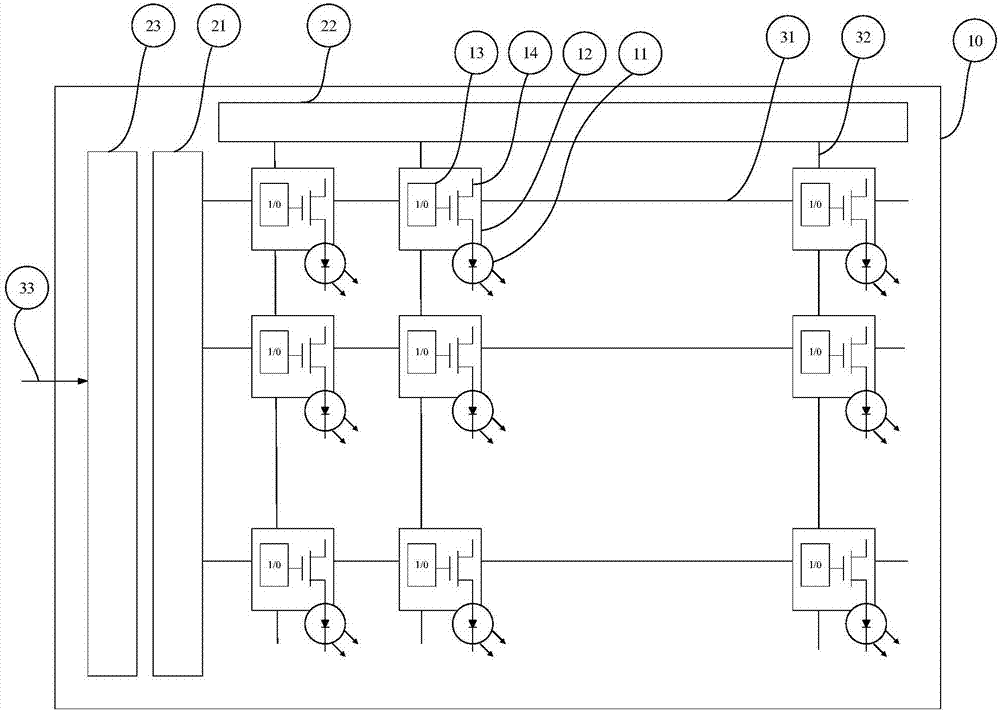
[0034] This embodiment discloses a digitally driven semiconductor display device, such as figure 1 As shown, it includes a silicon substrate 10 and micro light emitting diodes 11 fabricated in an array on the silicon substrate 10. A pixel circuit 12 is integrated in the silicon substrate 10 for driving the micro light emitting diodes 11. The pixel circuit 12 includes The metal-oxide semiconductor field effect transistor; the pixel circuit 12 and the micro light emitting diode 11 have a one-to-one correspondence; the silicon substrate 10 is preferably a single crystal silicon wafer or a cut single crystal silicon chip.

[0035] The micro light emitting diode 11 comprises a first electrode, a multi-layer non-organic compound and a second electrode, and the non-organic compound is composed of Ga, As, In, Al, Se, Zn, Si, P, N or C elements and can be Doping, the compounds are preferably GaAs, GaAsP, AlGaAs, AlGaInP, GaInN, AlGaP, AlGaN, GaP:ZnO, InGaN, GaN, GaP, ZnSe, Al 2 o 3 ,...

Embodiment 2

[0043] This embodiment is basically the same as Embodiment 1, the difference is that the micro light emitting diode 11 is a horizontal structure, which is characterized in that the two electrodes (the first electrode 43 and the second electrode 42) of the micro light emitting diode 11 are in a multilayer The same side of the non-organic compound layer 41 (light-emitting layer), such as Figure 4 As shown, the first electrode 43 is connected to the pixel circuit 12 through the through hole 44, and the second electrode 42 is connected to the pixel circuit 12 through the through hole 45, and the first electrode 43 and the second electrode 42 are conductive metal.

[0044] Further, the multilayer non-organic compound layer 41 preferably at least includes a bottom-up (or top-down) N-type doped layer (such as n-GaN), an MQW layer (multiple quantum well), a P-type doped layer (such as p-GaN), or include more layers to optimize performance. Furthermore, the micro light emitting diode...

Embodiment 3

[0052] This embodiment is basically the same as Embodiment 1, except that the distance between the micro-LEDs 11 is not greater than 20 μm, preferably 5-10 μm. The current of 11 is 0.1 μA to 30 μA, preferably 1˜5 μA.


PUM


Abstract

The invention discloses a digitally driven semiconductor display device which at least comprises a silicon substrate, and micro light emitting diodes that are manufactured on the silicon substrate and are arranged in an array. Furthermore each micro light emitting diode at least comprises a first electrode, a plurality of non-organic compound layers and a second electrode. The pixel circuit at least comprises a binary-value storage unit and a driving transistor. The driving transistor is an N-type or P-type metal-oxide semiconductor field effect transistor and only works in an on state or an off state. One end of the micro light emitting diode is connected with the source electrode or drain electrode of the driving transistor, and the other end is connected with a power supply, ground or a negative power supply. The light emitting brightness of the micro light emitting diode is in direct ratio with on time of the driving transistor in unit time. The gray scale generating mode of a display device is digital pulse width modulation. The digital pulse width modulation manner is subfield or subspace. The binary-value storage unit is arranged in a first voltage region, and the driving transistor is arranged in a second voltage region.

Description

technical field [0001] The invention relates to the field of semiconductor display devices, in particular to a digitally driven micro light-emitting diode semiconductor display device. Background technique [0002] Light-emitting diode (LED) display technology based on non-organic light-emitting materials has been widely used in various industries. Most of the existing LEDs are based on sapphire, with a single pixel pitch of more than 100 microns, and are mainly used for medium and large-sized screens. In the field of wearable near-eye display and projection display, displays with smaller physical area, higher integration and higher resolution are expected. Existing LED microdisplays based on monocrystalline silicon are still in the experimental stage, and the pixel pitch is more than 30 microns, which cannot well meet the above requirements. Further, the existing silicon-based LED driving technology follows the liquid crystal on silicon (LCOS) or organic light-emitting-on...

Claims


Application Information

Patent Timeline
Patent Type & Authority Applications(China)
IPC IPC(8): G09G3/32
CPCG09G3/32
Inventor 季渊刘万林黄舒平
Owner 南京昀光科技有限公司
Why Eureka
Try Eureka