Method for preparing single-electron transistor by assembling gold particles on PS microsphere template

A single-electron transistor, gold particle technology, applied in circuits, electrical components, semiconductor devices, etc., can solve the problem of inability to precisely control the size of Coulomb island assembly and positioning of the potential barrier between Coulomb islands and electrodes, so as to facilitate integrated batch preparation, reduce Difficulty, the effect of improving consistency

Pending Publication Date: 2017-07-07
NAT UNIV OF DEFENSE TECH
View PDF10 Cites 6 Cited by
  • Summary
  • Abstract
  • Description
  • Claims
  • Application Information

AI Technical Summary

Problems solved by technology

[0007] The purpose of the present invention is to propose a method for preparing single-electron transistors by assembling gold particles with a PS microsphere template, so as to overcome the deficiencies in the existing preparation methods, such as the size of the potential barrier between the Coulomb island and the electrode and the inability to accurately control the assembly and positioning of the Coulomb island, which is significant. Reduce the difficulty of preparing single-electron transistors and improve the consistency of performance of batch-fabricated single-electron transistors

Method used


Image

  • Method for preparing single-electron transistor by assembling gold particles on PS microsphere template
  • Method for preparing single-electron transistor by assembling gold particles on PS microsphere template
  • Method for preparing single-electron transistor by assembling gold particles on PS microsphere template

Examples


Embodiment Construction

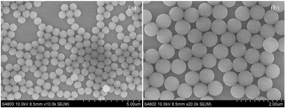
[0064] The invention utilizes the PS microsphere monolayer film to assemble the gold nanoparticle array to realize the precise control of the Coulomb island size, and its array arrangement is convenient for positioning and integration during processing; the thickness of the barrier layer is precisely controlled by atomic layer deposition technology; the present invention The technical difficulty of the invention is low, the feasibility is high, and a room-temperature single-electron transistor can be prepared.

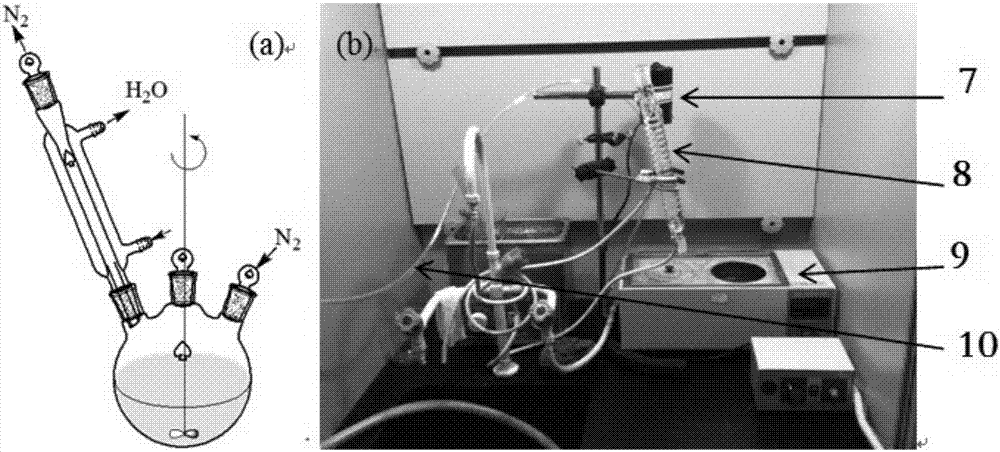
[0065] Below in conjunction with accompanying drawing, the concrete implementation of technical scheme of the present invention is described in further detail:

[0066] Such as Figure 14 As shown, the single-electron transistor of the present invention is mainly composed of a silicon substrate, a source, a drain, a gate, a barrier layer, a Coulomb island, and a protective layer, and is integrated on a silicon dioxide substrate, which is made of thermally oxidized pre...


PUM

PropertyMeasurementUnit
Thicknessaaaaaaaaaa
Thicknessaaaaaaaaaa
Thicknessaaaaaaaaaa

Abstract

The invention relates to a method for preparing a single-electron transistor by assembling gold particles on a PS microsphere template. According to the method, a silicon dioxide substrate is formed on the surface of a silicon base sheet; a coulomb island and an electrode are arranged on the silicon dioxide substrate in an integrated manner; an evenly and compactly-arranged PS microsphere single-layer film template is prepared on the silicon dioxide substrate; an electric beam evaporation coating method is utilized to plate a gold film on the surface of the PS microsphere single-layer film template; a chemical etching method and post-treatment are adopted, so that a gold nanoparticle array is obtained; an aluminum oxide barrier layer is formed on the gold nanoparticle array by using atomic layer deposition; the electrode is prepared by using electron beam exposure, electron beam evaporation coating and / or peeling methods; and an aluminum oxide protective layer is prepared on the electrode and the aluminum oxide barrier layer through using atomic layer deposition. The coulomb island is a size-controllable array, and therefore, positioning and batch preparation can be facilitated; and the size of the barrier between the coulomb island and the electrode can be precisely controlled. The method can be widely applied to fields such as photon, electronics, environment and security fields.

Description

technical field [0001] The invention relates to the technical field of nanoelectronic devices, in particular to a method for preparing a single-electron transistor by assembling a gold nanoparticle array with a PS microsphere monolayer film template. The PS is polystyrene. The gold particles are gold nanoparticles. Background technique [0002] In 1985, Likharev et al. of the former Soviet State Moscow University proposed the concept of single electrons for the first time. They predicted that it would be possible to control the movement of a single electron in and out of the Coulomb island, and this phenomenon would continue to increase as the size of the Coulomb island decreased, providing a physical basis for the fabrication of single-electron devices with potential applications. Among the current major single-electron devices, single-electron transistors have attracted much attention due to their advantages such as small size, high switching speed, and low power consump...

Claims


Application Information

Patent Timeline
IPC IPC(8): H01L21/335B82B3/00
CPCH01L29/66439B82B3/00
Inventor 方靖岳王飞孙佳雨江盼盼刘哲方涛张学骜秦石乔
Owner NAT UNIV OF DEFENSE TECH
Why Eureka
Try Eureka