A kind of wafer temporary bonding method

A temporary bonding, wafer technology, applied in semiconductor devices, electrical components, circuits, etc., can solve the problems of cumbersome bonding process steps, wafer warpage, etc., to reduce risks, avoid warpage, and reduce process steps. Effect

Active Publication Date: 2020-03-27
INST OF MICROELECTRONICS CHINESE ACAD OF SCI
View PDF3 Cites 0 Cited by
  • Summary
  • Abstract
  • Description
  • Claims
  • Application Information

AI Technical Summary

Problems solved by technology

[0005] In view of this, the present invention provides a temporary wafer bonding method to solve the problem of cumbersome round bonding process steps in the prior art and easily cause wafer warping

Method used


Image

  • A kind of wafer temporary bonding method
  • A kind of wafer temporary bonding method
  • A kind of wafer temporary bonding method

Examples


Embodiment Construction

[0032] The following will clearly and completely describe the technical solutions in the embodiments of the present invention with reference to the accompanying drawings in the embodiments of the present invention. Obviously, the described embodiments are only some, not all, embodiments of the present invention. Based on the embodiments of the present invention, all other embodiments obtained by persons of ordinary skill in the art without making creative efforts belong to the protection scope of the present invention.

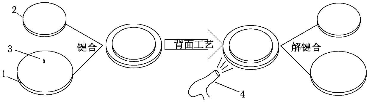
[0033] The typical temporary bonding process flow in the prior art is: the carrier wafer and / or the device wafer are spin-coated with a layer of bonding adhesive, and then the two wafers are transferred to the bonding chamber and placed in the bond In the center of the cavity, after raising the temperature, bonding is performed in a vacuum. After temporary bonding, the device wafer is subjected to backside processing, such as thinning, etching, etc., and then ...


PUM


Abstract

The invention discloses a wafer temporary bonding method which comprises the steps of supplying and cleaning a device wafer and a glass slide; dripping liquid on the glass slide and / or the device wafer; forming a bonded member through the glass slide and the device wafer by means of surface tension of the liquid; performing back surface processing on the device wafer in the bonded member; and debonding the glass slide and the device wafer. According to the wafer temporary bonding method provided by the invention, the device wafer is temporarily bonded with the glass slide by means of a surface tension effect of the liquid, and processes such as high-temperature processing or drying are not required, thereby reducing processes in wafer temporary bonding, preventing wafer warpage caused by high-temperature processing or a drying process, and reducing a wafer warpage risk.

Description

technical field [0001] The invention belongs to the technical field of semiconductor manufacturing, in particular to a wafer temporary bonding method. Background technique [0002] As new semiconductor products have higher and higher requirements for the integration and function of various components, the traditional two-dimensional integrated circuit has been difficult to meet the demand. Therefore, a new technology, three-dimensional integrated circuit (3DIC) has emerged, and its main principle It is to improve the integration of chips or various electronic components by stacking wafers and wafers (Wafer to Wafer) or chips and wafers (Chip to Wafer) on top of each other. In the 3DIC process, the wafer needs to be thinned, one is to reduce the thickness of the package, and the other is to expose the through-hole (Via) metal plug used to connect the upper and lower wafers through thinning. [0003] However, due to the reduction of mechanical strength and the increase of war...

Claims


Application Information

Patent Timeline
Patent Type & Authority Patents(China)
IPC IPC(8): H01L21/683
CPCH01L21/6835H01L2221/68381
Inventor 刘艳松赵超丁明正李俊峰
Owner INST OF MICROELECTRONICS CHINESE ACAD OF SCI
Why Eureka
Try Eureka