A kind of preparation method of nanocrystalline silicon thin film solar cell

A technology of solar cells and nanocrystalline silicon, applied in the field of solar cells, can solve problems such as ineffective conversion of electric energy, and achieve the effects of improving photoelectric conversion efficiency, improving stability and reducing light absorption loss

Active Publication Date: 2018-02-27
ZHEJIANG NORMAL UNIVERSITY
View PDF5 Cites 0 Cited by
  • Summary
  • Abstract
  • Description
  • Claims
  • Application Information

AI Technical Summary

Problems solved by technology

[0003] Due to the wide distribution of the spectral energy range of sunlight, a single semiconductor material can only absorb photons whose energy is greater than the bandgap width of the material, and the excess photon energy beyond the bandgap width is dissipated by heat and cannot be effectively absorbed. converted into electrical energy
In a p-i-n thin-film solar cell, if the active layer (i layer, intrinsic layer) of the cell is composed of a multilayer thin film with a tapered bandgap, then the sunlight with a shorter wavelength can be absorbed by the intrinsic layer with a wide bandgap, while the long-wavelength Longer sunlight can be transmitted and absorbed by the intrinsic layer with a smaller bandgap width, which may maximize the photoelectric conversion efficiency of the cell

Method used


Image

  • A kind of preparation method of nanocrystalline silicon thin film solar cell
  • A kind of preparation method of nanocrystalline silicon thin film solar cell

Examples


Embodiment Construction

[0015] In order to make the object, technical solution and advantages of the present invention clearer, the present invention will be further described in detail below in conjunction with the accompanying drawings and embodiments. It should be understood that the specific embodiments described here are only used to explain the present invention, not to limit the present invention.

[0016] The present invention will be further described below in conjunction with the accompanying drawings and embodiments.

[0017] 1.1 Main raw materials

[0018] ITO conductive glass: area ~4.0×4.0 cm 2 , sheet resistance ~15 Ω, light transmittance ³90%, Luoyang Longgan Glass Co., Ltd.;

[0019] Silane, phosphine, borane, carbon dioxide, hydrogen and other growth gas sources: purity greater than 99.995%, Dalian Date Gas Co., Ltd.;

[0020] 1.2 Main production equipment

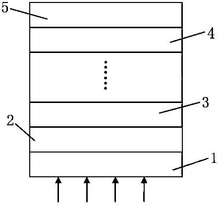
[0021] Plasma Chemical Vapor Deposition (PECVD) system: the vacuum chamber is composed of 4 independent vacuum chambers in...


PUM

PropertyMeasurementUnit
electrical conductivityaaaaaaaaaa

Abstract

The present invention discloses a method for manufacturing a nano-crystalline silicon thin-film solar cell. According to the technical scheme of the invention, the advantages of regulating and controlling the preparation process parameters of a nano-crystalline silicon thin film, changing the bandgap width of the nano-crystalline silicon thin film, adopting the nano-crystalline silicon thin film with the bandgap width thereof to be gradually changed, changing the light absorption of a cell, adopting the microcrystalline silicon oxide as a window layer, reducing the light absorption loss of the non-active layer of the cell, and maximally improving the photoelectric conversion efficiency of the cell are realized. A silicon-based thin-film cell of nano silicon / n-type nanocrystalline silicon / ITO conductive glass is prepared on a glass substrate, wherein the structure of the silicon-based thin-film cell is composed of a silver electrode / p-type microcrystalline silicon oxide / gradually changed bandgap. The photoelectric conversion efficiency is 9.05%. Compared with an amorphous silicon thin-film cell, the stability of the cell is greatly improved.

Description

technical field [0001] The invention belongs to the technical field of solar cells, and in particular relates to a method for preparing a nanocrystalline silicon thin-film solar cell with an adjustable band gap in which microcrystalline silicon oxide is a window layer. Background technique [0002] At present, three types of thin-film batteries, cadmium telluride, copper indium gallium selenide (CIGS), and silicon-based (amorphous silicon, microcrystalline silicon, etc.) represent the mainstream of the thin-film photovoltaic market. Compared with other types of thin-film batteries, silicon-based thin-film solar cells are still relatively low. However, due to the abundance of raw materials for silicon-based thin-film batteries in nature, the development of low-temperature plasma chemical vapor deposition (PECVD) technology is relatively mature. , it is easy to realize large-scale and automatic production, and it is compatible with the current mainstream semiconductor industry...

Claims


Application Information

Patent Timeline
Patent Type & Authority Patents(China)
IPC IPC(8): H01L31/18
CPCH01L31/18Y02P70/50
Inventor 黄仕华
Owner ZHEJIANG NORMAL UNIVERSITY
Why Eureka
Try Eureka