Semiconductor substrate, three-dimensional package chip and through-silicon via packaging method
A packaging method and a technology of through-silicon vias, which are applied in semiconductor devices, semiconductor/solid-state device manufacturing, semiconductor/solid-state device components, etc., can solve problems such as inconsistent thermal expansion coefficients, time-consuming manufacturing processes, and chip failures, etc., to improve the quality of finished products efficiency, prolong life, and simplify the manufacturing process
- Summary
- Abstract
- Description
- Claims
- Application Information
AI Technical Summary
Problems solved by technology
Method used
Image


Examples
Embodiment 1
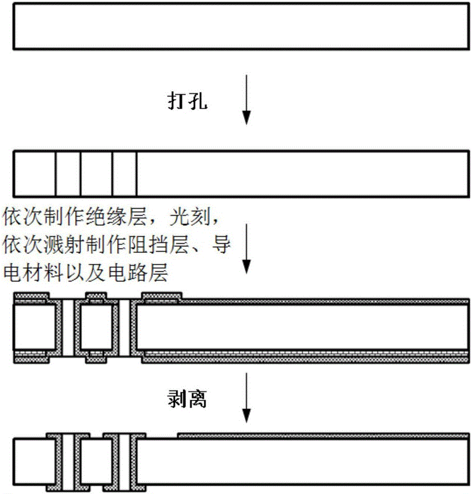
[0035] The preparation method of the semiconductor substrate of embodiment 1 is as image 3As shown, due to the improvement of the TSV packaging method, the process flow includes drilling, sequentially making insulating layers, photolithography, sequentially sputtering to make barrier layers, conductive materials and circuit layers, and stripping. Compared with the prior art, polishing is omitted process.
[0036] Such as Figure 4a As shown, it is a schematic diagram of the TSV (through-silicon via) pad array in Example 1. The size of the pad is 140 μm×140 μm, and each pad is distributed with a 7×7 square array of TSVs, and the diameter of each TSV hole is 10 μm. The pitch is 20 μm, the depth is 100 μm, and the thickness of the semiconductor base substrate where the TSV hole is located is 100 μm, such as Figure 4b shown. Each TSV is filled with copper rings by double-sided magnetron sputtering. Magnetron sputtering FHR equipment is used. The vacuum degree is 2E-7mbar, the...
Embodiment 2
[0038] For semiconductor substrates that are not suitable for thinning, due to the large depth of the semiconductor substrate and the limited TSV aspect ratio (generally not exceeding 10:1), the TSV aperture is usually large. The thickness of the semiconductor substrate in this embodiment is 600 μm, and the TSV aperture is 60 μm, such as Figure 5a shown. Due to the limitations of sputtering itself (cost and equipment performance), the thickness of the sputtered metal layer generally does not exceed 2 μm, and if sputtering is still used for copper filling at this time, the TSV copper filling rate may be less than 12.9%, resulting in semiconductor The electrical conductivity of the substrate is insufficient.
[0039] Therefore, for the preparation of this kind of chip, the filling method of electroplating is still used. For the TSV with a pore size of 60 μm, if electroplating is used for filling, since the copper layer is also grown on the surface of the chip when the TSV is e...
Embodiment 9
[0044] Filling TSVs by evaporation is similar to sputtering. The difference is that the sidewall attachment efficiency of evaporation is not as high as that of sputtering, and it is only suitable for filling TSVs with low aspect ratios. However, the advantage of evaporation is that it can achieve larger batches of processing technology. The equipment can realize the processing of multiple wafers at a time, and the cost is relatively low. For example, the diameter of TSV is 20 μm, the depth is 100 μm, and the aspect ratio is only 5:1. At this time, the electron beam evaporation process can be used to evaporate the copper layer on both sides in large quantities, using the COOKE electron beam evaporation table, and the evaporation rate is 20A / s , the pre-evaporation power is 45%, the evaporation power is 60%, and each side is evaporated for 3 hours to form a copper layer with a thickness of 2 μm, so that the thickness of the copper layer on the side wall of the TSV is 4 μm, and th...
PUM
 Abstract
Description
Claims
Application Information
 - R&D
- Intellectual Property
- Life Sciences
- Materials
- Tech Scout
- Unparalleled Data Quality
- Higher Quality Content
- 60% Fewer Hallucinations
Browse by: Latest US Patents, China's latest patents, Technical Efficacy Thesaurus, Application Domain, Technology Topic, Popular Technical Reports.
© 2025 PatSnap. All rights reserved.Legal|Privacy policy|Modern Slavery Act Transparency Statement|Sitemap|About US| Contact US: help@patsnap.com