Adhesive sheet for copper-clad laminate
A bonding sheet and copper-clad laminate technology, which is applied in the field of communication materials, can solve the problems of narrow adjustable range of dielectric properties of bonding sheets, increased production difficulty, and small usable range, achieving uniform thickness and easy control, and low production cost. Low, boost adjustable range of effects
- Summary
- Abstract
- Description
- Claims
- Application Information
AI Technical Summary
Problems solved by technology
Method used
Image
Examples
Embodiment 1
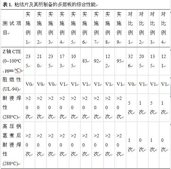
[0021] Weigh 75 parts of PTFE (Japan Daikin PTFE M-18), 75 parts of PFA (DuPont Teflon PFA340), 70 parts of titanium dioxide (Tianjin Zhongzheng Huamei Technology) and 1 part of KH550 (Nanjing Shuguang Chemical General Factory), and mix them evenly with a high-speed mixer After that, at 360 o C. 120 kg / cm 2 After hot pressing and sintering for 24 hours, the bonding sheet is obtained by turning, and its thickness is about 0.095~0.105mm; the bonding sheet is pressed with the PTFE board at high temperature to obtain a multi-layer board, and then at 300 o C for 5 minutes, repeated 5 times, it can be observed that the multi-layer board has no blisters, no delamination, and almost no change in appearance, strength and toughness.
Embodiment 2
[0023]Weigh 150 parts of PTFE (Japan Daikin PTFE M-18), 10 parts of PFA (DuPont Teflon PFA340), 80 parts of titanium dioxide (Tianjin Zhongzheng Huamei Technology) and 2 parts of KH550 (Nanjing Shuguang Chemical General Factory), and mix them evenly with a high-speed mixer After that, at 430 o C. 200 kg / cm 2 After hot pressing and sintering for 24 hours, the bonding sheet is obtained by turning, and its thickness is about 0.095~0.105mm; the bonding sheet is pressed with the PTFE board at high temperature to obtain a multi-layer board, and then at 300 o C for 5 minutes, repeated 5 times, it can be observed that the multi-layer board has no blisters, no delamination, and almost no change in appearance, strength and toughness.
Embodiment 3
[0025] Weigh 110 parts of PTFE (Japan Daikin PTFE L-5), 30 parts of FEP (Japan Daikin Neoflon FEP NC-1539), 10 parts of ethylene-tetrafluoroethylene copolymer (ETFE) (DuPont Teflon Tefzel ETFE750), 50 parts Titanium dioxide (Tianjin Zhongzheng Huamei Technology), 30 parts of silicon dioxide (Xinyi Hongrun) and 1 part of KH550 (Nanjing Shuguang Chemical General Factory), after being uniformly mixed by a high-speed mixer, at 380 o C. 150 kg / cm 2 After hot pressing and sintering for 24 hours, the bonding sheet is obtained by turning, and its thickness is about 0.0105~0.115mm; the bonding sheet is pressed with the PTFE board at high temperature to obtain a multi-layer board, and then at 300 o C for 5 minutes, repeated 5 times, it can be observed that the multi-layer board has no blisters, no delamination, and almost no change in appearance, strength and toughness.
PUM
| Property | Measurement | Unit |
|---|---|---|
| Thickness | aaaaa | aaaaa |
| Thickness | aaaaa | aaaaa |
| Thickness | aaaaa | aaaaa |
Abstract
Description
Claims
Application Information
 - R&D
- Intellectual Property
- Life Sciences
- Materials
- Tech Scout
- Unparalleled Data Quality
- Higher Quality Content
- 60% Fewer Hallucinations
Browse by: Latest US Patents, China's latest patents, Technical Efficacy Thesaurus, Application Domain, Technology Topic, Popular Technical Reports.
© 2025 PatSnap. All rights reserved.Legal|Privacy policy|Modern Slavery Act Transparency Statement|Sitemap|About US| Contact US: help@patsnap.com

