Formation method and structure of a double gate fin field effect transistor

A fin-type field effect and transistor technology, which is applied in semiconductor devices, semiconductor/solid-state device manufacturing, electrical components, etc., can solve problems such as high leakage and differences between the upper and lower parts of fins, so as to improve device performance, reduce leakage, and change threshold voltage Effect

Active Publication Date: 2019-05-14
SHANGHAI HUALI MICROELECTRONICS CORP
View PDF4 Cites 0 Cited by
  • Summary
  • Abstract
  • Description
  • Claims
  • Application Information

AI Technical Summary

Problems solved by technology

[0005] However, in the actual manufacturing process, on the one hand, because the ion implantation process is difficult to distribute evenly in the vertical direction of the fin (fin), even if there are differences between the upper and lower parts of the fin
On the other hand, the effective channel bottom leakage of the fin is higher

Method used


Image

  • Formation method and structure of a double gate fin field effect transistor
  • Formation method and structure of a double gate fin field effect transistor
  • Formation method and structure of a double gate fin field effect transistor

Examples


Embodiment Construction

[0047] Embodiments embodying the features and advantages of the present invention will be described in detail in the following description. It should be understood that the invention can have various changes in different examples without departing from the scope of the invention, and that the descriptions and illustrations therein are illustrative in nature rather than limiting the invention.

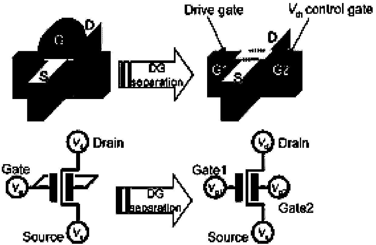
[0048] The process method of increasing the ILD filling window with the adjustable control gate of the present invention will be further described in detail with reference to the accompanying drawings.

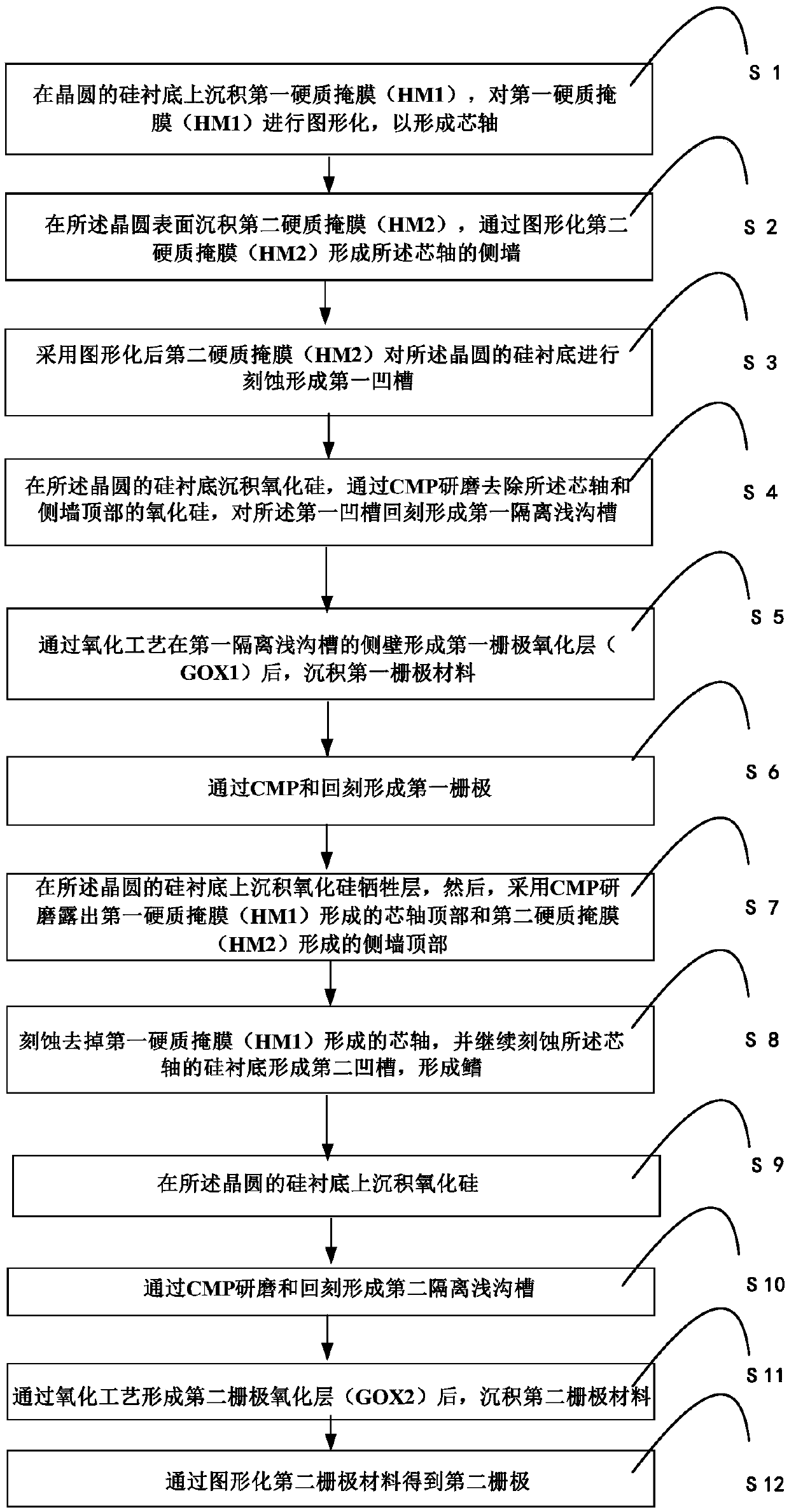
[0049] see figure 2 , figure 2 It is a schematic flow chart of a double-gate fin field effect transistor in an embodiment of the present invention, and the forming steps of the method may include:

[0050] Step S1 : Depositing a first hard mask HM1 on the silicon substrate Si of the wafer, and patterning the first hard mask HM1 to form mandrels.

[0051] see image 3 , image 3 I...


PUM


Abstract

The invention provides a double gate fin type field effect transistor forming method and a structure thereof. One side of the lower part of a fin forms a gate which serves as a control gate, and the upper part of the fin forms the other gate which serves as a drive gate. The method can reduce electricity leakage of the effective channel bottom part of the fin, can effectively change a threshold voltage of the drive gate by adjusting the thickness of the control gate, and can increase device properties.

Description

technical field [0001] The invention relates to the field of integrated circuit manufacturing, in particular to a method for forming a double gate fin field effect transistor and its structure. Background technique [0002] In the process of manufacturing FinFET, the ion implantation process is the main link. The ion implantation process is a material modification method that introduces dopant atoms into a solid. Simply put, the process of ion implantation is to irradiate the atoms to be doped with accelerated ions in a vacuum system (implantation ) solid material to form a surface layer (implanted layer) with specific properties in the selected (i.e. injected) area. [0003] At present, a variety of double gate fin field effect transistor (double gate) structures have been proposed. The source (Source) and drain (Drain) parts of these double gate fin field effect transistors look like fish fins, and the gate The pole (gate) is different from the previous circuits on the s...

Claims


Application Information

Patent Timeline
Patent Type & Authority Patents(China)
IPC IPC(8): H01L29/78H01L29/423H01L21/336
CPCH01L29/4232H01L29/66795H01L29/7855
Inventor 鲍宇
Owner SHANGHAI HUALI MICROELECTRONICS CORP
Why Eureka
Try Eureka