Mask for fixing conductive ball and manufacturing method thereof

A manufacturing method and technology of conductive balls, applied in the field of masks, can solve the problems of insufficient mechanical strength or chemical resistance, large thickness deviation of spacers, unstable precipitation of electroplating, etc. Deformation and reduction of defects

Active Publication Date: 2016-10-26
PROCESS LAB MICRON
View PDF8 Cites 1 Cited by
  • Summary
  • Abstract
  • Description
  • Claims
  • Application Information

AI Technical Summary

Problems solved by technology

[0008] Here, in the case of forming metal spacers by electrolytic plating, a photoresist patterning process such as a photosensitive dry film or a liquid resist or an electroforming process is performed by photolithography. Processes such as the photoresist film stripping process are complicated
In addition, there is a problem that if the design pattern becomes finer, the current density will be concentrated in the place where the photoresist is dense, so that the deposition of plating becomes unstable depending on the position, resulting in a large variation in the thickness of the spacer
In addition, also in the case of forming with a resin, since a photoresist coating process and a photoresist patterning process by photolithography are necessary, the process is relatively complicated, and it is difficult to Coated with a thinner thickness, the mechanical strength and chemical resistance are not sufficient
[0009] Furthermore, as described in Patent Document 3, when the spacer has a protruding shape such as a pillar shape, it has the following problems: it is easy to be damaged, and when cleaning the fixed surface of the metal mask, cleaning tools such as waste cloth Hooks easily to the struts so it's not easy to wipe down, etc.

Method used


Image

  • Mask for fixing conductive ball and manufacturing method thereof
  • Mask for fixing conductive ball and manufacturing method thereof
  • Mask for fixing conductive ball and manufacturing method thereof

Examples


Embodiment Construction

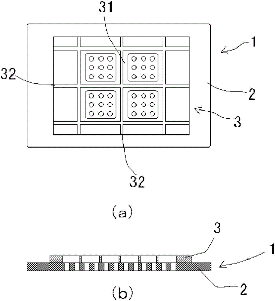
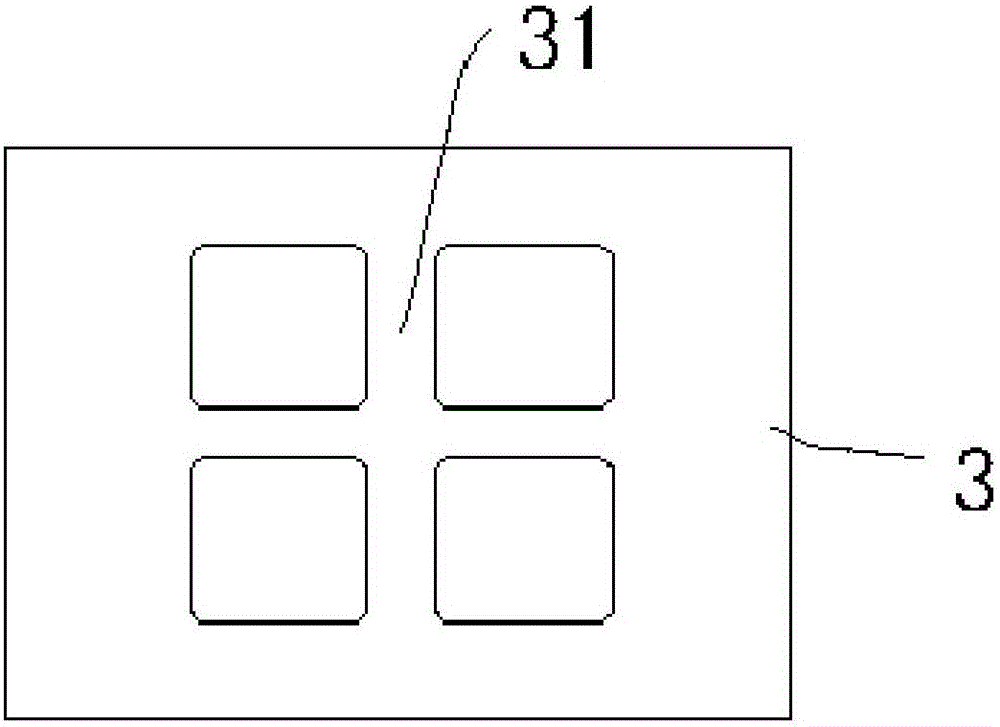
[0041]figure 1 It is a front view (a) and a cross-sectional view (b) of the conductive ball fixing mask 1 of the embodiment. First, the conductive ball fixing mask 1 roughly includes a metal mask (mask) 2 and a resin sheet (sheet) 3, and the metal mask 2 and the resin sheet 3 are bonded by an adhesive sheet (not shown).

[0042] The metal mask 2 is made of a metal thin plate such as nickel or stainless steel, and generally has a thickness of 0.015 mm to 0.2 mm, and an external dimension of a quadrilateral (square or rectangular) with a side of 100 mm to 600 mm. Here, the manufacturing method of the metal mask 2 includes an electrolytic plating method, an etching method, a laser processing method, etc. as described later, but any of them may be used in this embodiment.

[0043] In the surface of the metal mask 2, in order to allow conductive balls to penetrate, a plurality of The through hole is the opening 21. Here, in order to allow the conductive balls to be smoothly inse...


PUM


Abstract

A mask for fixing a conductive ball and a manufacturing method thereof are prvoided. The spacer for fixing a conductive ball is used for forming a bump on a substrate or a wafer. The mask has a spacer and is less likely to damage the workpiece. The thickness of the spacer is uniform throughout the mask, and is formed in a plurality of designs such as a planar shape and a linear shape, and is excellent in chemical resistance and mechanical strength. A resin thin plate such as polyimide is used as a spacer-forming member, and a spacer having a predetermined design pattern formed by ultraviolet rays is attached to a metal mask prepared by electrolytic plating or the like. Alternatively, the spacer may be processed in a state where the resin sheet is attached to the metal mask.

Description

technical field [0001] The invention relates to a mask used for fixing conductive balls to electrodes on workpieces such as substrates or wafers. Background technique [0002] In the semiconductor manufacturing process, when performing flip-chip mounting or forming bump electrodes on a silicon wafer, the following method is generally used: on the electrodes arranged in a predetermined pattern on a workpiece such as a substrate or a silicon wafer, fix the conductive material with solder or the like. Conductive balls made of non-conductive metals are subjected to a reflow process to melt solder and bonded to electrodes (for example, refer to Patent Document 1). [0003] Here, a stencil metal mask in which fine openings are formed on a thin metal plate is used as a jig for fixing the conductive balls. The openings are formed in a pattern corresponding to the electrodes on the workpiece, and are set so that when the metal mask is properly arranged relative to the workpiece, the...

Claims


Application Information

Patent Timeline
Patent Type & Authority Applications(China)
IPC IPC(8): H01L21/60
CPCH01L24/10H01L24/11H01L2224/1012
Inventor 谷口义博千叶秀贵
Owner PROCESS LAB MICRON
Why Eureka
Try Eureka