Silicon oxycarbide film and RRAM (resistive random access memory)
A technology of resistive memory and silicon oxycarbide, applied in electrical components and other directions, can solve the problems of unreported resistive memory of silicon oxycarbide, potential safety hazards, etc., and achieve the effects of optimizing resistive characteristics, reducing consumption, and simplifying design
- Summary
- Abstract
- Description
- Claims
- Application Information
AI Technical Summary
Problems solved by technology
Method used
Image
Examples
Embodiment 1
[0019] Embodiment one: device preparation
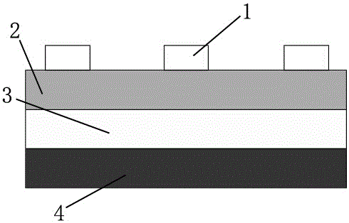
[0020] The schematic diagram of the cross-sectional structure of the resistive memory of the present invention is as follows: figure 1 As shown, the preparation process of the resistive variable memory of this example is described below in conjunction with the schematic cross-sectional structure.
[0021] 1. First, P-type heavily doped silicon wafers with a thickness of 500 μm (resistivity less than ) is cleaned using the RCA standard cleaning method in the IC process.
[0022] 2. Using radio frequency magnetron reactive sputtering 4H-SiC target with a purity of 99.5%, a resistive dielectric layer SiC with a thickness of about 20nm was prepared at room temperature x o y , where x=1.21, y=1.45. Parameters: background vacuum -4 , working pressure=0.5Pa, argon flow=30sccm, RF frequency=13.56MHz, RF power=100W, growth time=10min.
[0023] 3. Define the shape and size of the top electrode (a circle with a diameter of 1 mm) using a m...
Embodiment 2
[0026] Embodiment 2: Device detection
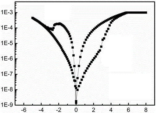
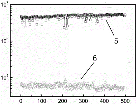
[0027] This embodiment tests the resistive switching characteristics of the resistive memory made in Example 1, and the test results are as follows figure 2 , image 3 and Figure 4 as shown, image 3 Among them, the abscissa represents the number of erasing and writing, the ordinate represents the resistance, the unit is ohm, 5 represents the high-resistance state curve, and 6 represents the low-resistance state curve; Figure 4 , the abscissa represents the retention time, in seconds, the ordinate represents the resistance, in ohms, 5 represents the high-resistance state curve, and 6 represents the low-resistance state curve.
[0028] Depend on figure 2 It can be seen that with the cycle of DC scanning voltage, the device Ag / SiC 1.21 o 1.45 / p + -The resistance of Si will change from high resistance state to low resistance state, reflecting the storage of data 0 and 1.
[0029] Depend on image 3 and Figure 4 It can be see...
Embodiment 3
[0030] Embodiment three: device preparation
[0031] This example uses the same method as Example 1 to prepare a resistive variable memory, and the prepared device has the same structure as Example 1, the difference is that the flow rate of argon gas is 29.9 sccm, and the flow rate of oxygen gas is 0.1 sccm, so that the resistance of this example is Variable dielectric layer SiC x o y x:y=0.72:1.76. The resistive switching characteristic test described in the second embodiment is carried out on the prepared device, and it is found that the device can well meet the requirement.
PUM
| Property | Measurement | Unit |
|---|---|---|
| thickness | aaaaa | aaaaa |
| thickness | aaaaa | aaaaa |
| thickness | aaaaa | aaaaa |
Abstract
Description
Claims
Application Information
 - R&D
- Intellectual Property
- Life Sciences
- Materials
- Tech Scout
- Unparalleled Data Quality
- Higher Quality Content
- 60% Fewer Hallucinations
Browse by: Latest US Patents, China's latest patents, Technical Efficacy Thesaurus, Application Domain, Technology Topic, Popular Technical Reports.
© 2025 PatSnap. All rights reserved.Legal|Privacy policy|Modern Slavery Act Transparency Statement|Sitemap|About US| Contact US: help@patsnap.com


