Gan thin film grown on yttrium aluminum garnet substrate and its preparation method and application

A technology of yttrium aluminum garnet and substrate, which is applied in the field of GaN thin film and its preparation, can solve problems such as heat accumulation, affecting device performance, and difficult chip heat discharge, so as to reduce the formation of dislocations and lattice mismatch Small, guaranteed lattice matching effect

Active Publication Date: 2018-09-28
HEYUAN CHOICORE PHOTOELECTRIC TECH CO LTD
View PDF4 Cites 0 Cited by
  • Summary
  • Abstract
  • Description
  • Claims
  • Application Information

AI Technical Summary

Problems solved by technology

However, due to the lattice mismatch between sapphire and GaN as high as 13.3%, resulting in a density of ~10 9 cm -2 dislocation defects, thereby reducing the carrier mobility of the material and shortening the carrier lifetime, which in turn affects the performance of GaN-based devices
Secondly, due to the low thermal conductivity of sapphire (25W / m K at 100°C), it is difficult to discharge the heat generated in the chip in time, resulting in heat accumulation, which reduces the internal quantum efficiency of the device and ultimately affects the performance of the device

Method used


Image

  • Gan thin film grown on yttrium aluminum garnet substrate and its preparation method and application
  • Gan thin film grown on yttrium aluminum garnet substrate and its preparation method and application
  • Gan thin film grown on yttrium aluminum garnet substrate and its preparation method and application

Examples


Embodiment 1

[0028] The GaN thin film grown on the yttrium aluminum garnet substrate, its preparation method comprises the following steps:

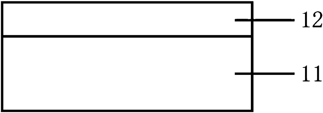
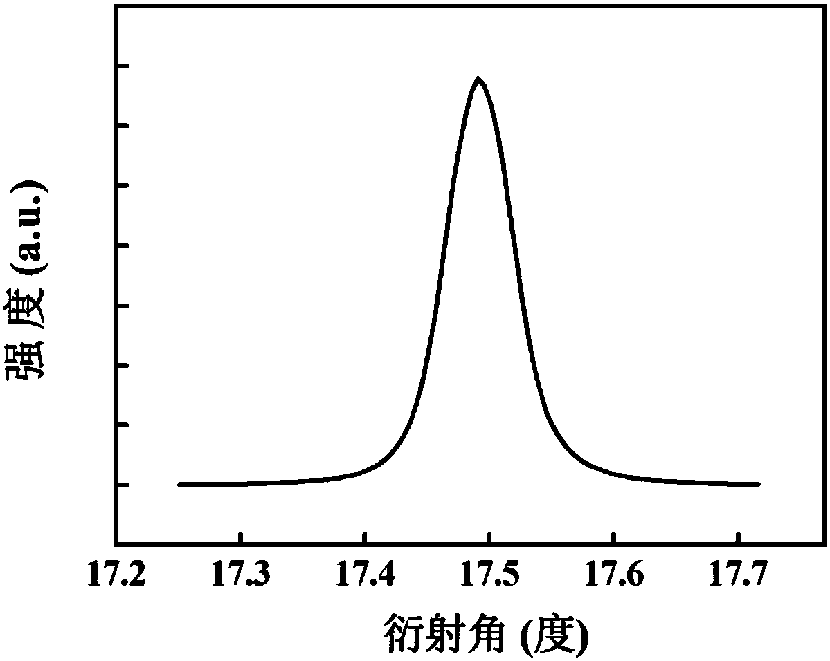
[0029] (1) Selection of the substrate and its crystal orientation: Y 3 Al 5 o 12 The substrate, with the (111) plane offset from the (100) plane by 0.5° as the epitaxial plane, the crystal epitaxial orientation relationship is: the (0001) plane of GaN is parallel to the Y 3 Al 5 o 12 (111) side;

[0030] (2)Y 3 Al 5 o 12 Substrate surface annealing treatment, the specific process is: Y 3 Al 5 o 12 Put the substrate into the reaction chamber, and perform in-situ annealing treatment in a nitrogen atmosphere at 800°C for 2 hours. The annealing treatment can make Y 3 Al 5 o 12 The substrate obtains an atomically flat surface;

[0031] (3) Epitaxial growth of GaN film: using pulsed laser deposition process, Y 3 Al 5 o 12 The substrate is kept at 400 °C and the pressure in the reaction chamber is 1.0 x 10 -3 A GaN film with a thickness of...

Embodiment 2

[0038] The GaN thin film grown on the yttrium aluminum garnet substrate, its preparation method comprises the following steps:

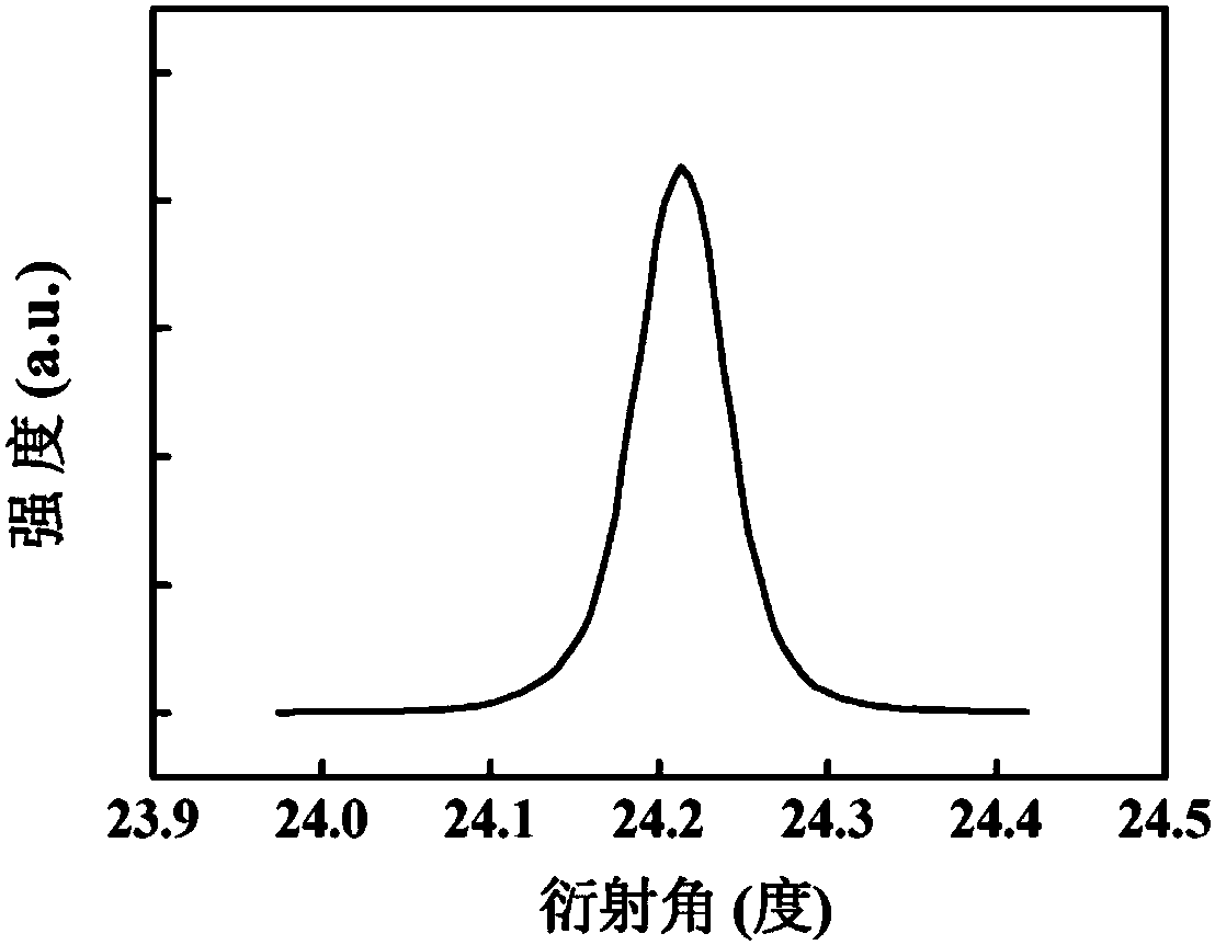
[0039] (1) Selection of the substrate and its crystal orientation: Y 3 Al 5 o 12 The substrate, with the (111) plane offset from the (100) plane by 1° as the epitaxial plane, the crystal epitaxial orientation relationship is: the (0001) plane of GaN is parallel to the Y 3 Al 5 o 12 (111) side;

[0040] (2)Y 3 Al 5 o 12 Substrate surface annealing treatment, the specific process is: Y 3 Al 5 o 12 The substrate was placed in the reaction chamber, and the Y 3 Al 5 o 12 The substrate is annealed in situ for 1h, and the annealing treatment can make Y 3 Al 5 o 12 The substrate obtains an atomically flat surface;

[0041] (3) Epitaxial growth of GaN film: using pulsed laser deposition process, Y 3 Al 5 o 12 The substrate is kept at 600 °C and the pressure in the reaction chamber is 6.0 x 10 -3 A GaN film with a thickness of 1000 nm was ...


PUM

PropertyMeasurementUnit
thicknessaaaaaaaaaa
thicknessaaaaaaaaaa
thicknessaaaaaaaaaa

Abstract

The invention discloses a GaN film growing on a yttrium aluminum garnet substrate. The GaN film growing on the yttrium aluminum garnet substrate comprises the yttrium aluminum garnet substrate and a GaN film, wherein the GaN film grows on the yttrium aluminum garnet substrate in an epitaxial mode; the yttrium aluminum garnet substrate takes a surface (111) deflecting from a surface (100) by 0.5 to 1 degree as an epitaxial surface, and the orientation relation between the yttrium aluminum garnet substrate and the GaN film is that a surface (0001) of the GaN film is parallel to a surface (111) of the yttrium aluminum garnet substrate. The crystal quality of the GaN film is good. The invention further discloses a preparation method of the GaN film growing on the yttrium aluminum garnet substrate. The preparation method is simple in technology and low in preparation cost. Besides, the GaN film growing on the yttrium aluminum garnet substrate is also applied to an LED device, a photoelectric detector and a solar battery device.

Description

technical field [0001] The invention relates to the technical field of GaN thin films, in particular to a GaN thin film grown on a yttrium aluminum garnet substrate and a preparation method and application thereof. Background technique [0002] Light-emitting diode (LED), as a new type of solid-state lighting source, is considered to be a green lighting source in the 21st century due to its advantages of low calorific value, low power consumption, fast response, long life, and small size. Facing the market demand for high-power lighting in the future, the luminous efficiency of LED still needs to be further improved if it is to be widely used on a large scale. At present, LED chips are mainly prepared by GaN material systems grown on sapphire substrates. However, due to the lattice mismatch between sapphire and GaN as high as 13.3%, resulting in a density of ~10 9 cm -2 The dislocation defects of the material reduce the carrier mobility of the material and shorten the car...

Claims


Application Information

Patent Timeline
Patent Type & Authority Patents(China)
IPC IPC(8): H01L21/02H01L31/18H01L33/00H01L29/04
CPCH01L21/0242H01L21/0254H01L21/0262H01L21/02694H01L29/045H01L31/1856H01L33/0075Y02E10/544Y02P70/50
Inventor 李国强
Owner HEYUAN CHOICORE PHOTOELECTRIC TECH CO LTD
Why Eureka
Try Eureka