Double split trench gate charge storage-type RC-IGBT and manufacturing method thereof
A charge storage and charge storage layer technology, applied in semiconductor/solid-state device manufacturing, circuits, electrical components, etc., can solve the compromise characteristics of switching losses affecting the turn-on voltage drop of devices, increase gate capacitance, and reduce device switching. speed etc.
- Summary
- Abstract
- Description
- Claims
- Application Information
AI Technical Summary
Problems solved by technology
Method used
Image
Examples
Embodiment 1
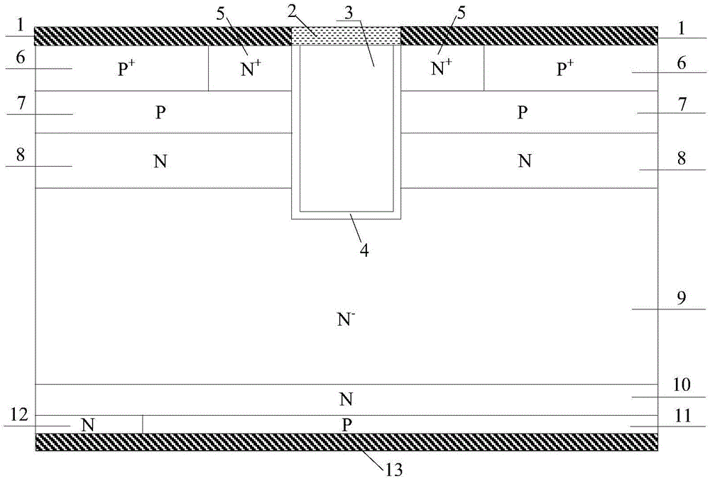
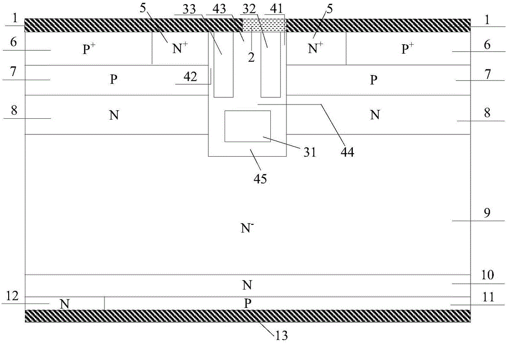
[0047] In this example, a double-split trench gate charge storage RC-IGBT, its cell structure is as follows figure 2 As shown, it includes: the back collector metal 13, the P-type collector region 11 and the N-type collector region 12 located on the back collector metal 13 and connected to it, and the P-type collector region 11 and the N-type collector region The N-type field stop layer 10 above and connected to the N-type field stop layer 10, the N-drift region 9 located on the N-type field stop layer 10 and connected to it; the compound double split trench located in the middle of the upper part of the N-drift region 9 and connected to it Structure: the N-type charge storage layer 8 located on both sides of the upper part of the N-drift region 9 and connected to it, the side wall of the N-type charge storage layer 8 is connected to the composite double split trench structure, and is located on the upper part of the N-type charge storage layer 8 The p-type base region 7 conn...
Embodiment 2
[0049] In this example, a double-split trench gate charge storage RC-IGBT, its cell structure is as follows image 3 As shown, different from Embodiment 1, the lower part of the side split electrode 33 directly extends to the upper surface of the bottom split electrode 31, so that the side split electrode 33 and the bottom split electrode 31 are directly connected to further reduce the gate capacitance of the device.
[0050] The specific implementation scheme of the process manufacturing method of the present invention is described by taking the double-split trench gate charge storage type RC-IGBT with a voltage level of 600V as an example, and the specific process manufacturing method is as follows:
[0051] Step 1: Select a doping concentration of 2×10 14 piece / cm 3 , a lightly doped FZ silicon wafer with a thickness of 300-600 microns is used to form the N-drift region 9 of the device; the N-type field stop layer 10 of the device is fabricated by ion-implanting N-type imp...
PUM
 Abstract
Description
Claims
Application Information
 - R&D
- Intellectual Property
- Life Sciences
- Materials
- Tech Scout
- Unparalleled Data Quality
- Higher Quality Content
- 60% Fewer Hallucinations
Browse by: Latest US Patents, China's latest patents, Technical Efficacy Thesaurus, Application Domain, Technology Topic, Popular Technical Reports.
© 2025 PatSnap. All rights reserved.Legal|Privacy policy|Modern Slavery Act Transparency Statement|Sitemap|About US| Contact US: help@patsnap.com


