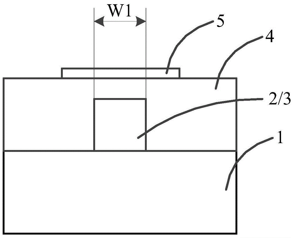
Organic-inorganic hybrid integrated thermo-optical modulation type grating and preparation method thereof
An integrated thermo-optic and modulation technology, applied in the direction of optical waveguide light guide, light guide, optics, etc., can solve the problem that the thermo-optic modulation effect of the full silica grating is not obvious, and achieve excellent transparency, low price, and high thermo-optic coefficient. Effect
- Summary
- Abstract
- Description
- Claims
- Application Information
AI Technical Summary
Problems solved by technology
Method used
Image
Examples
preparation example Construction
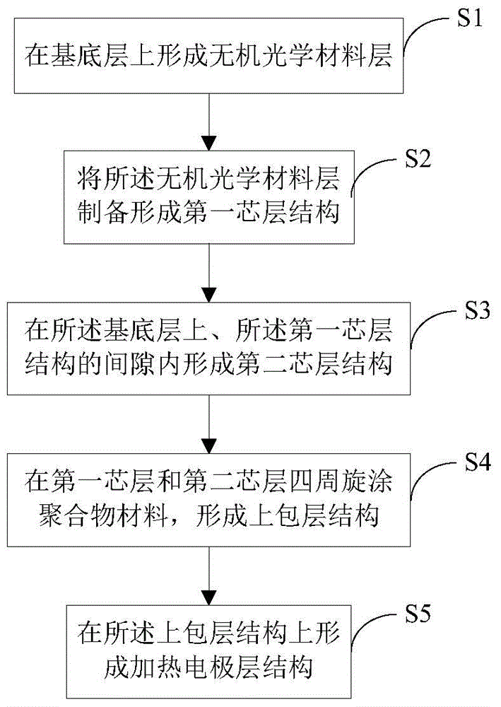
[0073] refer to image 3 , is a flowchart of a method for preparing an organic-inorganic hybrid integrated thermo-optic modulation grating according to another embodiment, and the preparation method includes the following steps:
[0074] Step S1: forming an inorganic optical material layer on the base layer.
[0075] Step S2: preparing the inorganic optical material layer to form a first core layer structure.
[0076] Step S3: forming a second core structure on the base layer and in the gap of the first core structure, the material of the second core structure includes an ultraviolet polymerized fluorinated polymer material, and the first The core layers and the second core layers are arranged alternately along the light propagation direction.
[0077] Step S4: Spin coating polymer material around the first core layer and the second core layer to form an upper cladding structure.
[0078] Step S5: forming a heating electrode layer structure on the upper cladding layer struc...
Embodiment approach
[0079] As a preferred embodiment, the method for preparing an organic-inorganic hybrid integrated thermo-optic modulation grating sequentially performs the following steps, and corresponding to the specific steps of the preparation method, the generation process of the organic-inorganic hybrid integrated thermo-optic modulation grating is as follows: Figure 4 shown.
[0080] The specific steps of forming an inorganic optical material layer on the base layer in the above step S1 include:
[0081] Step S11: growing a layer of inorganic optical material 2-1 on the base layer 1; preferably, the method of growing a layer of inorganic optical material 2-1 on the base layer 1 adopts plasma enhanced chemical vapor deposition. The base layer is made of silicon dioxide.
[0082] Step S12: Doping the inorganic optical material layer 2-1 with ions; preferably, germanium ions are used as the ions.
[0083] Step S13: annealing and hardening the ion-doped inorganic optical material layer....
PUM
 Abstract
Description
Claims
Application Information
 - R&D Engineer
- R&D Manager
- IP Professional
- Industry Leading Data Capabilities
- Powerful AI technology
- Patent DNA Extraction
Browse by: Latest US Patents, China's latest patents, Technical Efficacy Thesaurus, Application Domain, Technology Topic, Popular Technical Reports.
© 2024 PatSnap. All rights reserved.Legal|Privacy policy|Modern Slavery Act Transparency Statement|Sitemap|About US| Contact US: help@patsnap.com


