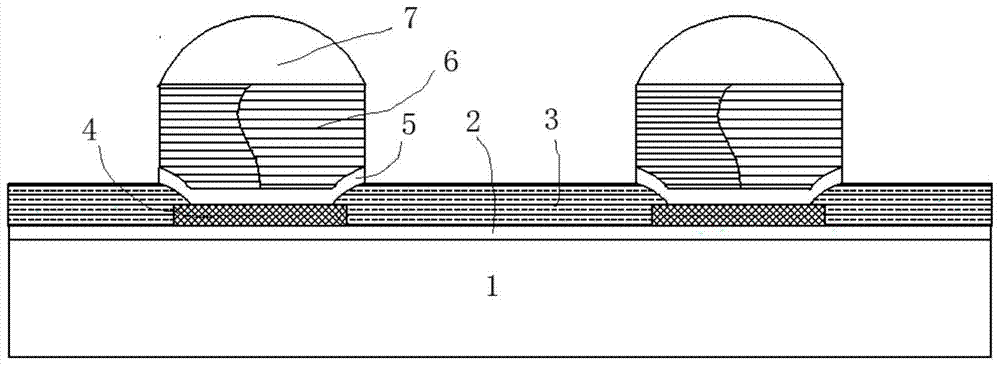
Directional growth copper pillar bump interconnection structure and preparation method thereof
A technology of interconnection structure and directional growth, applied in semiconductor/solid-state device manufacturing, electrical components, electrical solid-state devices, etc., to achieve the effect of improving interconnection performance and service reliability, realizing industrialization, and easy industrialization
- Summary
- Abstract
- Description
- Claims
- Application Information
AI Technical Summary
Problems solved by technology
Method used
Image
Examples
Embodiment 1
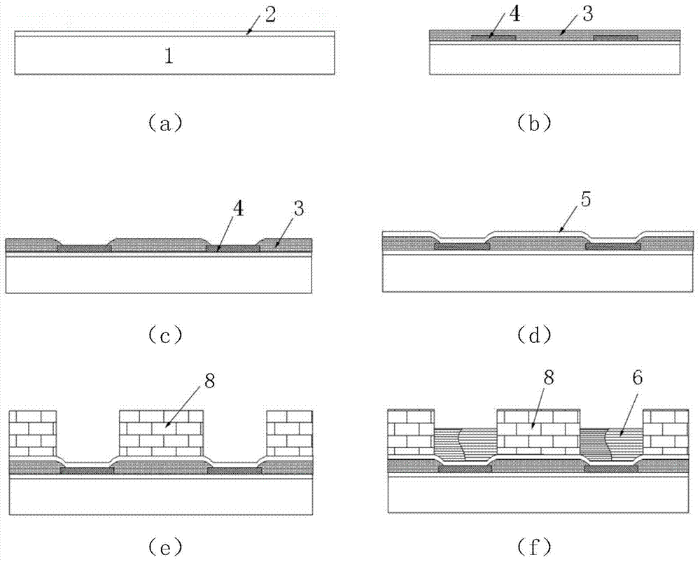
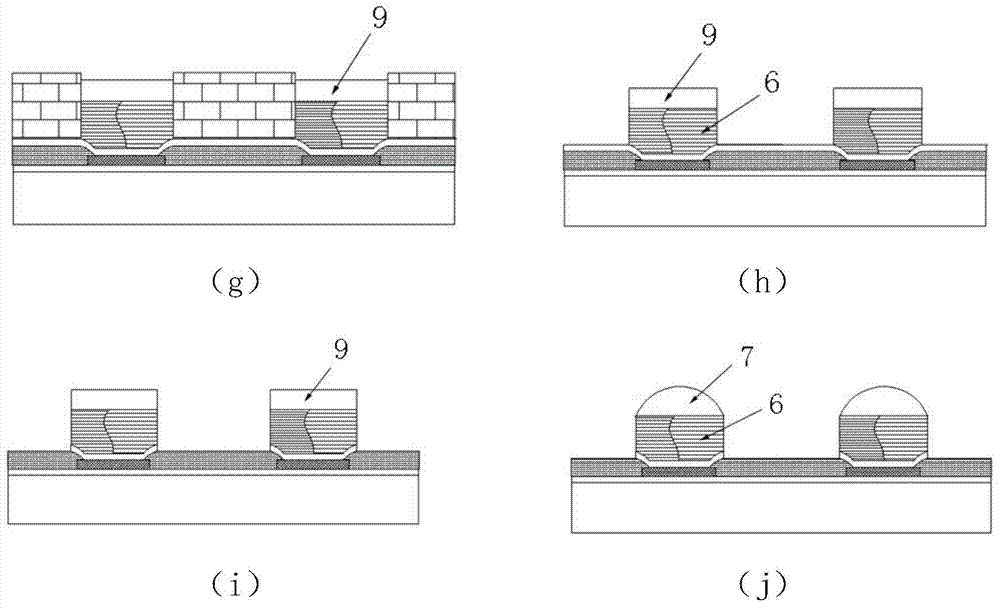
[0054] figure 2 It is a process flow chart for preparing a copper pillar bump interconnection structure of directional growth nano-twinned copper in the present invention, and the process steps are:
[0055] (1) Prepare the wafer substrate 1 with insulating layer 2, such as figure 2 (a), arranging a metal disc 4 on the insulating layer 2; or directly using a chip on which a metal disc and interconnection lines have been arranged as a substrate;
[0056] (2) deposit dielectric layer 3 on insulating layer 2 and metal plate 4, as figure 2 (b), selectively masking and etching the dielectric layer makes the surface of the metal disk 4 exposed in the window of the dielectric layer 3, such as figure 2 (c);
[0057] (3) Deposit seed layer 5 on dielectric layer 3 and exposed metal disk 4, as figure 2 (d); The method of depositing the seed layer is physical vapor deposition (PVD) or sputtering, etc., the thickness of the seed layer is about 200nm, and the materials are Ti and C...
Embodiment 2
[0068] This embodiment is a preparation process for a copper pillar bump interconnection structure of directional growth nano-twinned copper, which is different from Embodiment 1 in that: step (5) in the process of direct current electroplating copper pillars: the electroplating solution is composed of: copper sulfate 200g / L, methanesulfonic acid 40mL / L, sodium chloride 30ppm (calculated according to the chlorine content in sodium chloride), polyethyleneimine 5ppm, gelatin 20ppm, and the rest is water; the electroplating anode plate is phosphor copper plate, phosphor copper plate The P element content in the medium is 0.03‐0.075wt.%, and the current density is 40mA / cm 2 , Electromagnetic stirring is used in the electroplating process to ensure that the concentration in the plating solution is uniform.
[0069] The cross-sectional structure of the copper pillars in the copper pillar bump interconnection structure obtained in this embodiment is analyzed, and the result is the sa...
PUM
| Property | Measurement | Unit |
|---|---|---|
| thickness | aaaaa | aaaaa |
| thickness | aaaaa | aaaaa |
| thickness | aaaaa | aaaaa |
Abstract
Description
Claims
Application Information
 - R&D
- Intellectual Property
- Life Sciences
- Materials
- Tech Scout
- Unparalleled Data Quality
- Higher Quality Content
- 60% Fewer Hallucinations
Browse by: Latest US Patents, China's latest patents, Technical Efficacy Thesaurus, Application Domain, Technology Topic, Popular Technical Reports.
© 2025 PatSnap. All rights reserved.Legal|Privacy policy|Modern Slavery Act Transparency Statement|Sitemap|About US| Contact US: help@patsnap.com


