Impedance matched electrical interconnect using dielectric compounds

a technology of dielectric compounds and electrical interconnections, which is applied in the direction of electrical apparatus, semiconductor devices, semiconductor/solid-state device details, etc., can solve the problems of degrading the electrical performance of the packaged ic device, and achieve the effect of reducing or eliminating electromagnetic wave propagation discontinuities and improving the electrical performance of the ic devi

Inactive Publication Date: 2005-09-06
IBM CORP
View PDF3 Cites 0 Cited by
  • Summary
  • Abstract
  • Description
  • Claims
  • Application Information

AI Technical Summary

Benefits of technology

[0005]The present invention provides techniques for controlling an impedance of electrical interconnects associated with an IC device (or alternative interconnect structure) and eliminating or reducing electromagnetic wave propagation discontinuities, thereby improving the electrical performance of the IC device, especially at very high operating frequencies (e.g., 10 GHz and above). The invention involves the use of dielectric compounds placed on one or more electrical interconnects associated, for example, with the IC package. The interconnects can be wire / ribbon bonds, leadframe pins, etc., which tend to introduce discontinuities and parasitic inductance that can degrade the electrical performance of the packaged IC device.
[0006]In accordance with one aspect of the invention, an improved electrical interconnect is formed wherein a dielectric material having a controllable characteristic is applied to at least a portion of the interconnect. An impedance associated with the electrical interconnect is affected, at least in part, by the controllable characteristic of the dielectric material. The controllable characteristic is selectively adjustable so that the impedance of the electrical interconnect is substantially matched to at least one impedance at first and second ends of the interconnect. In this manner, an electrical discontinuity between the first and second ends of the interconnect is reduced, thereby improving an electrical performance of the interconnect.

Problems solved by technology

The interconnects can be wire / ribbon bonds, leadframe pins, etc., which tend to introduce discontinuities and parasitic inductance that can degrade the electrical performance of the packaged IC device.

Method used


Image

  • Impedance matched electrical interconnect using dielectric compounds
  • Impedance matched electrical interconnect using dielectric compounds
  • Impedance matched electrical interconnect using dielectric compounds

Examples


Embodiment Construction

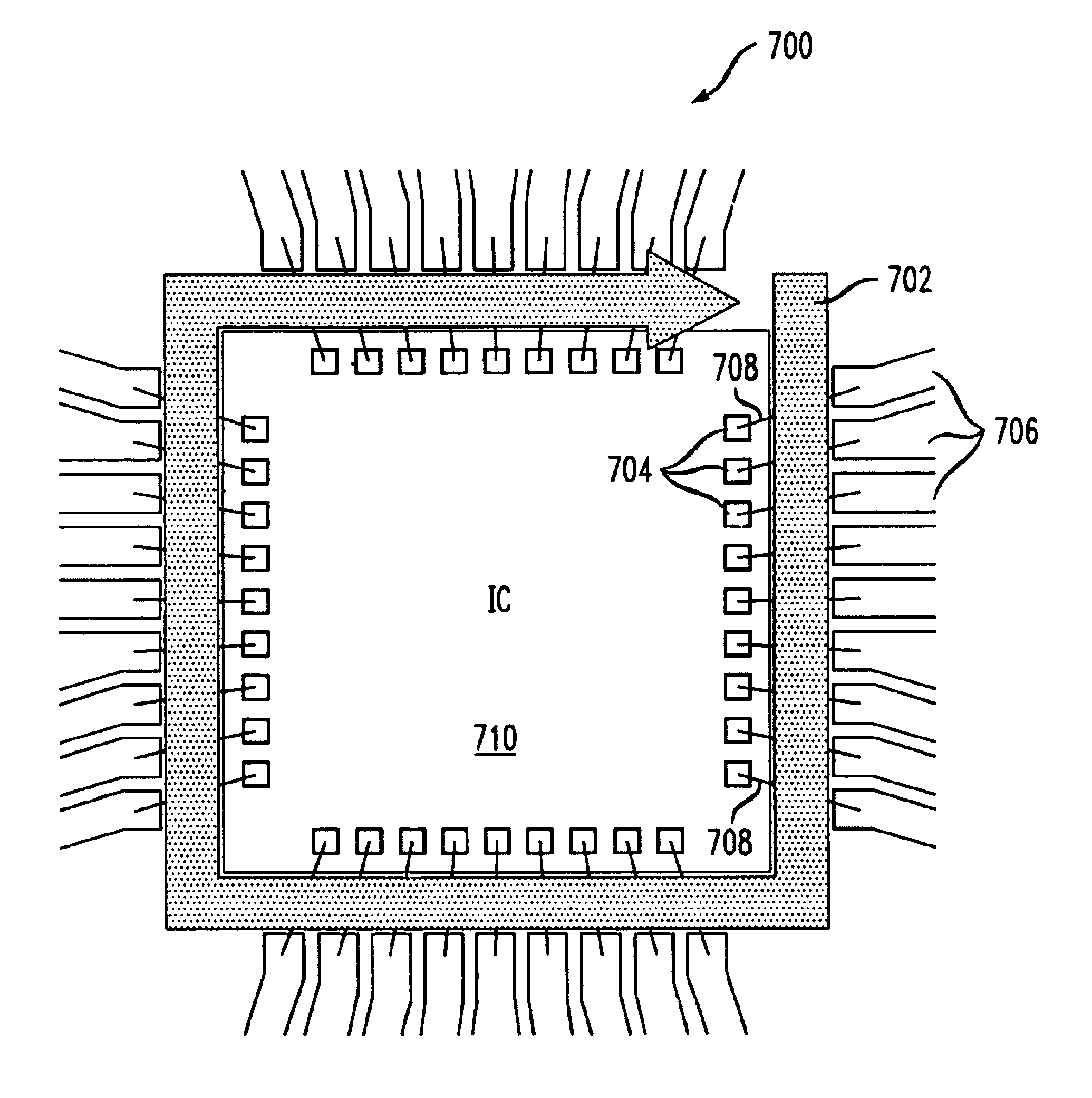
[0017]The present invention, which relates to improved electrical interconnects, will be described herein in the context of an IC device. It is to be appreciated, however, that the techniques of the present invention are not limited to IC devices. Rather, the techniques of the invention may be generally employed for tuning an impedance associated with an electrical interconnect such that the impedance of the interconnect is substantially matched to at least one impedance at respective ends of the interconnect. Moreover, the techniques of the present invention may be utilized, for example, with a flexible circuit manufacturing process. In this manner, undesirable effects due, at least in part, to discontinuities and / or parasitic inductances associated with the interconnect can be minimized.

[0018]As previously stated, the present invention provides techniques for controlling an impedance of electrical interconnects associated with an IC device, or alternative interconnect structure, s...


PUM


Abstract

An improved electrical interconnect is formed wherein a dielectric material having a controllable characteristic is applied to at least a portion of the interconnect. The controllable characteristic of the dielectric material is selectively adjustable so that the impedance of the electrical interconnect is substantially matched to at least one impedance at first and second ends of the interconnect. In this manner, an electrical discontinuity between the first and second ends of the electrical interconnect is reduced, thereby improving an electrical performance of the interconnect.

Description

FIELD OF THE INVENTION[0001]The present invention relates generally to electrical interconnections, and more particularly relates to techniques for controlling an impedance of an electrical interconnect, particularly in an integrated circuit (IC) device.BACKGROUND OF THE INVENTION[0002]Conventional IC devices generally include a semiconductor die having a plurality of bond pads thereon, a leadframe mechanically connected to the die, and bond wires which electrically couple the bond pads of the die with pins on the leadframe. The semiconductor die, bond wires and at least a portion of the leadframe are then surrounded with an encapsulation material, such as plastic, to help ensure the structural rigidity of the IC device.[0003]With the continual push to increase the operating frequency of electronic devices, electrical interconnects, comprising, for example, wire / ribbon bonds, leadframe pins, etc., become a primary bottleneck in the electrical performance of a semiconductor device. T...

Claims


Application Information

Patent Timeline
Patent Type & Authority Patents(United States)
IPC IPC(8): H01L23/48H01L23/58H01L23/495H01L23/64
CPCH01L23/4952H01L23/645H01L2223/6627H01L2224/49171H01L2924/1903H01L2924/30107H01L2924/3011H01L24/49H01L2924/30111H01L24/48H01L2224/05599H01L2224/45099H01L2224/85399H01L2924/00014H01L2924/14H01L2924/181H01L2924/00H01L2224/45015H01L2924/207
Inventor OPRYSKO, MODEST M.SHAN, LEITREWHELLA, JEANNINE M.
Owner IBM CORP
Why Eureka
Try Eureka