Method for forming metal interconnect structure

A metal interconnection structure and metal layer technology, which is applied in the manufacturing of electrical components, circuits, semiconductor/solid-state devices, etc., to achieve the effects of small damage, reduced damage, and reduced by-products

Active Publication Date: 2018-11-16
SEMICON MFG INT (SHANGHAI) CORP
View PDF8 Cites 0 Cited by
  • Summary
  • Abstract
  • Description
  • Claims
  • Application Information

AI Technical Summary

Problems solved by technology

In the metal interconnect structure formed by the existing metal interconnect structure formation method, the problem of electromigration has become increasingly prominent

Method used


Image

  • Method for forming metal interconnect structure
  • Method for forming metal interconnect structure
  • Method for forming metal interconnect structure

Examples


Embodiment Construction

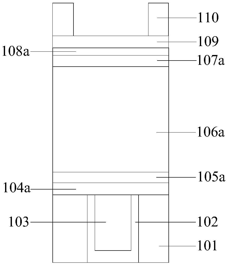
[0031] In the conventional method, after the contact hole is formed, a repair process is performed. However, in the existing methods, repairing treatment is usually carried out at a temperature of 20° C. to 60° C. The temperature condition of 20°C to 60°C is based on two considerations: on the one hand, it is generally believed that repairing at a higher temperature will have adverse effects on other semiconductor structures; on the other hand, the higher the temperature, the corresponding process The thermal budget is higher, resulting in increased process costs. Therefore, the existing methods usually carry out repair treatment at slightly higher than room temperature. Moreover, generally those skilled in the art do not think that the repair process after forming the contact hole is related to the electromigration problem of the finally formed metal interconnection structure.

[0032] However, after research and analysis, the present invention increases the temperature use...


PUM


Abstract

The invention discloses a formation method of a metal interconnection structure. The method comprises the following steps: providing a semiconductor substrate; forming a metal layer on the semiconductor substrate; forming a dielectric layer on the metal layer; forming a contact hole in the dielectric layer, the bottom of the contact hole exposing the metal layer; performing restoration processing on the side wall of the contact hole, a temperature scope employed by the restoration processing ranging from 70 DEG C to 400 DEG C; and filling the contact hole by use of a metal material. The metal interconnection structure formed by using the formation method has better performance, reduces the RC delay of the metal interconnection structure and remarkably improves the electromigration problem of the metal interconnection structure.

Description

technical field [0001] The invention relates to the field of semiconductor manufacturing, in particular to a method for forming a metal interconnection structure. Background technique [0002] With the rapid development of semiconductor manufacturing technology, in order to achieve faster computing speed, larger data storage capacity and more functions of semiconductor devices, semiconductor chips are developing towards higher integration. The higher the integration degree of the semiconductor chip, the smaller the critical dimension (CD) of the semiconductor device. Correspondingly, the size of the metal interconnection structure in the semiconductor chip is also continuously reduced. [0003] With the gradual reduction of the feature size, the influence of the RC delay of the metal interconnection structure on the operating speed of the device becomes more and more obvious. How to reduce the RC delay is one of the hot issues studied by those skilled in the art. More impo...

Claims


Application Information

Patent Timeline
Patent Type & Authority Patents(China)
IPC IPC(8): H01L21/768
Inventor 张海洋周俊卿
Owner SEMICON MFG INT (SHANGHAI) CORP
Why Eureka
Try Eureka