Acidic texturing liquid for silicon wafer pyramid texturing, texturing method and silicon wafer formed in texturing manner through adoption of texturing method
A technology of texturing liquid and pyramid, which is applied in the field of solar cells, can solve the problems of long reaction time and achieve the effects of shortening time, reducing cost and simplifying operation process
- Summary
- Abstract
- Description
- Claims
- Application Information
AI Technical Summary
Problems solved by technology
Method used
Image
Examples
Embodiment 1
[0060] 1) Surface cleaning steps
[0061] Take a P-type silicon wafer with a size of 156cm×156cm (resistivity 1Ω·cm~3Ω·cm), put it in acetone and ultrasonically clean it for 5 minutes, put it in ethanol for 5 minutes, and then place it in sulfuric acid solution and In the mixed liquid of hydrogen peroxide solution (the concentration of sulfuric acid solution is 70wt.%, the concentration of hydrogen peroxide solution is 35wt.%, the volume ratio of sulfuric acid solution and hydrogen peroxide solution is 3:1), heat and boil the silicon chip and keep it for 0.5 hours, and finally Clean it ultrasonically with deionized water.
[0062] 2) Etching step
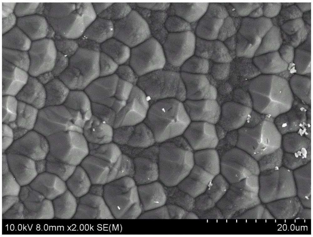
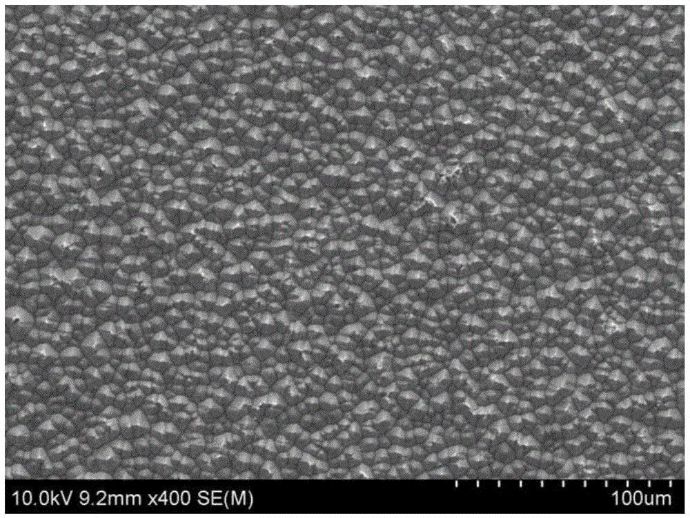
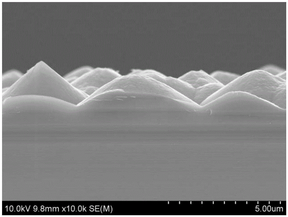
[0063] Immerse the pre-cleaned and water-washed silicon wafers in step 1) in the acidic texturing solution consisting of copper nitrate, hydrofluoric acid and nitric acid (wherein the concentration of copper nitrate is 8.0mmol / L, and the concentration of hydrofluoric acid is 4.8 mol / L, the concentration of nitric acid is 1.2 mol / L...
Embodiment 2
[0067] 1) Surface cleaning steps
[0068] Take a P-type silicon wafer with a size of 156cm×156cm (resistivity 1Ω·cm~3Ω·cm), put it in acetone and ultrasonically clean it for 5 minutes, put it in ethanol for 5 minutes, and then place it in sulfuric acid solution and In the mixed solution of hydrogen peroxide solution (the concentration of sulfuric acid solution is 70wt.%, the concentration of hydrogen peroxide solution is 35wt.%, the volume ratio of sulfuric acid solution and hydrogen peroxide solution is 3:1), silicon wafer is heated and boiled and kept for 0.5 hours, and finally Clean it ultrasonically with deionized water.
[0069] 2) Etching step
[0070] Immerse the pre-cleaned and water-washed silicon wafers in step 1) in an acidic texturing solution consisting of copper nitrate, hydrofluoric acid and nitric acid (wherein the concentration of copper nitrate is 10mmol / L, and the concentration of hydrofluoric acid is 4.8mol / L, the concentration of nitric acid is 1.2mol / L...
Embodiment 3
[0075] 1) Surface cleaning steps
[0076] Take a P-type silicon wafer with a size of 156cm×156cm (resistivity 1Ω·cm~3Ω·cm), put it in acetone and ultrasonically clean it for 5 minutes, put it in ethanol for 5 minutes, and then place it in sulfur solution and In the mixed liquid of hydrogen peroxide solution (the concentration of sulfuric acid solution is 70wt.%, the concentration of hydrogen peroxide solution is 35wt.%, the volume ratio of sulfuric acid solution and hydrogen peroxide solution is 3:1), heat and boil the silicon chip and keep it for 0.5 hours, and finally Clean it ultrasonically with deionized water.
[0077] 2) Etching step
[0078] Immerse the pre-cleaned and water-washed silicon wafers in step 1) in an acidic texturing solution consisting of copper nitrate, hydrofluoric acid and nitric acid (wherein the concentration of copper nitrate is 10mmol / L, and the concentration of hydrofluoric acid is 4.8mol / L, the concentration of nitric acid is 1.8mol / L), at room...
PUM
| Property | Measurement | Unit |
|---|---|---|
| Height | aaaaa | aaaaa |
| Resistivity | aaaaa | aaaaa |
| Size | aaaaa | aaaaa |
Abstract
Description
Claims
Application Information
 - R&D
- Intellectual Property
- Life Sciences
- Materials
- Tech Scout
- Unparalleled Data Quality
- Higher Quality Content
- 60% Fewer Hallucinations
Browse by: Latest US Patents, China's latest patents, Technical Efficacy Thesaurus, Application Domain, Technology Topic, Popular Technical Reports.
© 2025 PatSnap. All rights reserved.Legal|Privacy policy|Modern Slavery Act Transparency Statement|Sitemap|About US| Contact US: help@patsnap.com


