Bipolar transistor epitaxial wafer manufacturing method adopting varied temperature and varied doping flow
A technology of bipolar transistors and manufacturing methods, applied in semiconductor/solid-state device manufacturing, electrical components, circuits, etc., can solve the problem of low growth rate growth temperature, influence of epitaxial layer doping concentration and vertical carrier distribution, and yield rate reduce the problem, achieve the effect of increasing the growth temperature and suppressing the graphics drift
- Summary
- Abstract
- Description
- Claims
- Application Information
AI Technical Summary
Problems solved by technology
Method used
Image
Examples
Embodiment 1
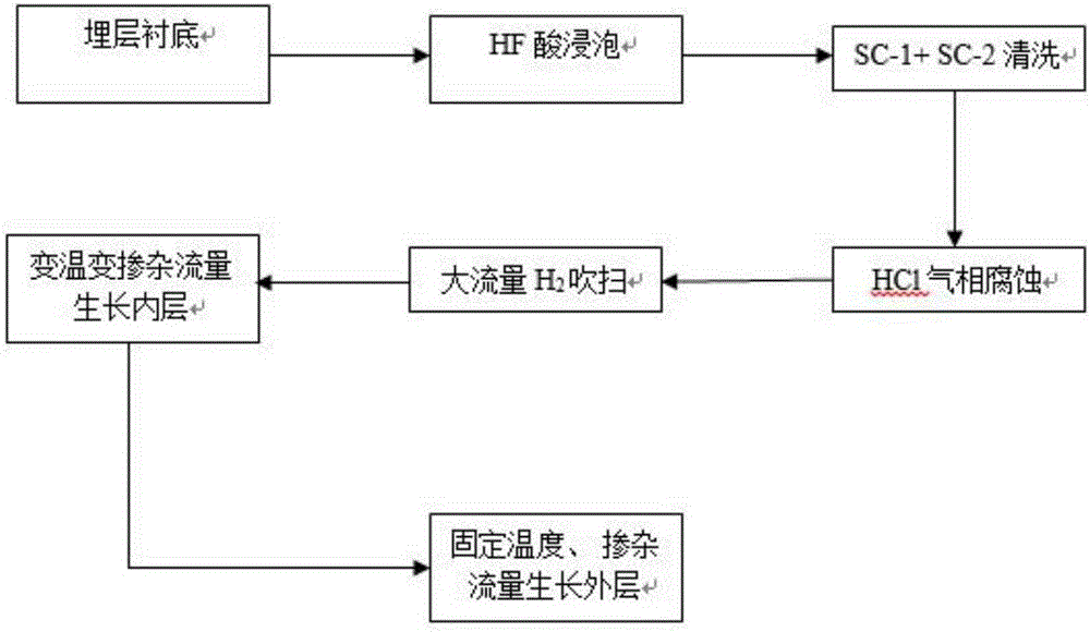
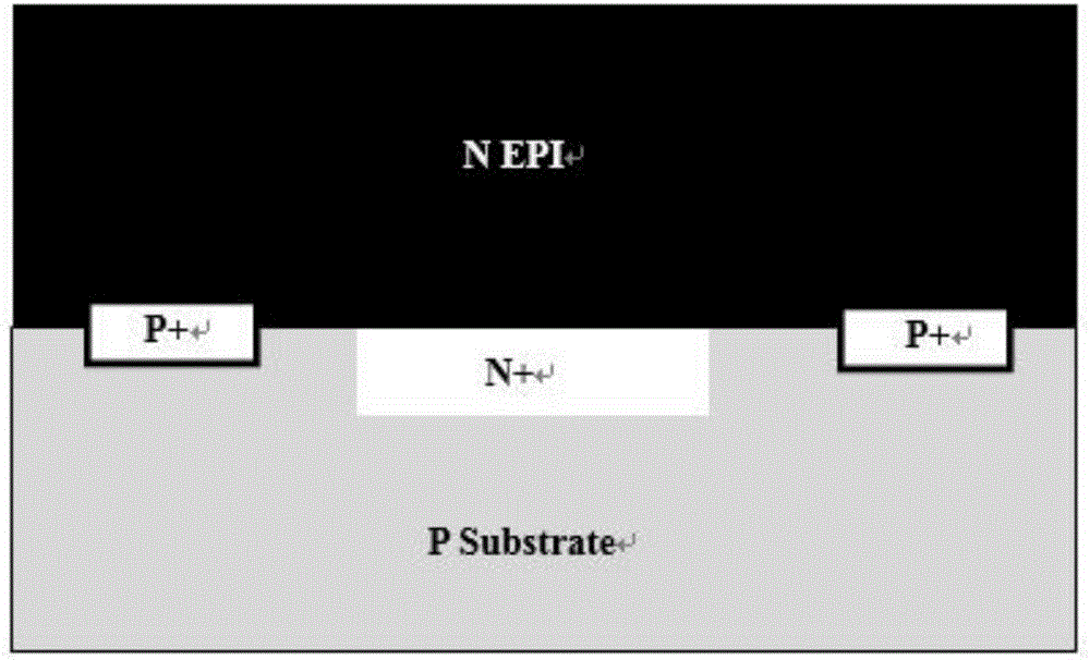
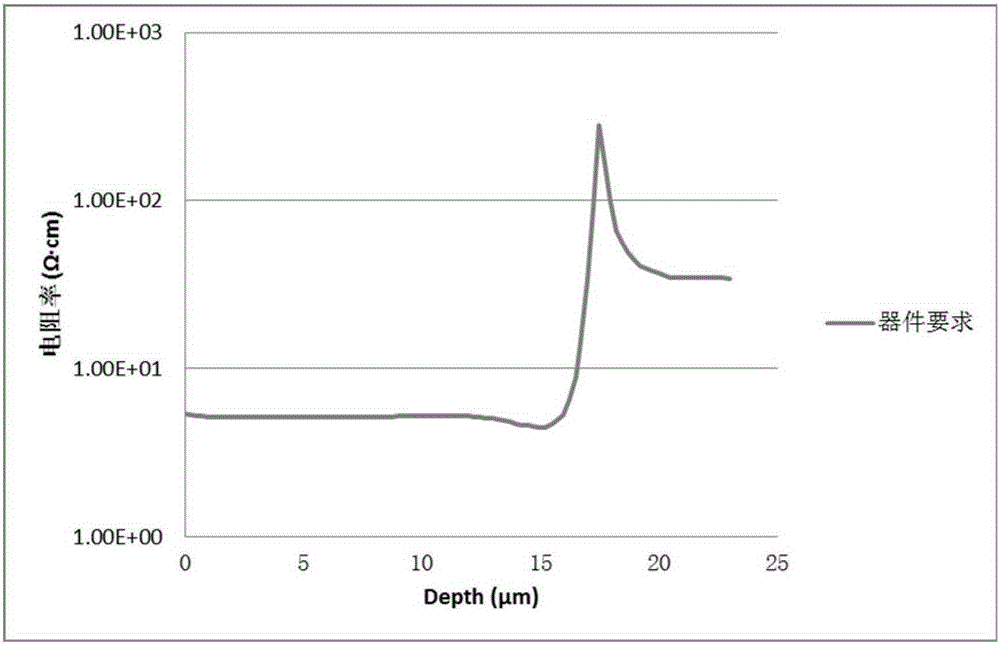
[0026] Embodiment 1: The epitaxial equipment used in this embodiment is: PE2061S barrel type epitaxial furnace of Italian LPE Company. The specific steps of the method adopted in this embodiment are as follows: figure 1 As shown, the device material structure involved in this embodiment is as figure 2 Shown: the diameter is 6 inches, the P-type conductive substrate, the crystal orientation is , the resistivity is 8-13Ω·cm, the square resistance of the B buried layer area is 90Ω / □ (ohm per square), and the substrate is fabricated For N+ and P+ buried layers, the N-type impurity is Sb, the P-type impurity is B, the resistivity of the N-type epitaxial layer is 7Ω·cm, and the thickness is 18.5μm. The requirements for the vertical distribution of the resistivity of the epitaxial layer are as follows image 3 shown.
[0027] 1. Epitaxial substrate preparation: After forming a buried layer on the substrate surface through oxidation, photolithography, diffusion and other processes,...
Embodiment 2
[0033] Embodiment 2: The epitaxial equipment used in this embodiment is: PE2061S barrel type epitaxial furnace of Italian LPE Company. The specific steps of the method adopted in this embodiment are as follows: figure 1 Shown:
[0034] 1. Epitaxial substrate preparation: After forming a buried layer on the substrate surface through oxidation, photolithography, diffusion and other processes, there are often oxide layers and impurities on the substrate surface. In order to obtain a clean epitaxial substrate, the oxide layer and impurities need to be removed. Impurities. In the present invention, HF acid is used to remove the oxide layer on the surface of the buried layer substrate, and then the surface of the buried layer substrate is cleaned with silicon wafer cleaning solution SC-1 and silicon wafer cleaning solution SC-2.
[0035]2. Epitaxial vapor phase etching: Before epitaxy, in-situ HCl etching on the surface of silicon wafers is an important means to remove contaminati...
Embodiment 3
[0039] Embodiment 3: The epitaxial equipment used in this embodiment is: PE2061S barrel type epitaxial furnace of Italian LPE Company. The specific steps of the method adopted in this embodiment are as follows: figure 1 Shown:
[0040] 1. Epitaxial substrate preparation: After forming a buried layer on the substrate surface through oxidation, photolithography, diffusion and other processes, there are often oxide layers and impurities on the substrate surface. In order to obtain a clean epitaxial substrate, the oxide layer and impurities need to be removed. Impurities. In the present invention, HF acid is used to remove the oxide layer on the surface of the buried layer substrate, and then the surface of the buried layer substrate is cleaned with silicon wafer cleaning solution SC-1 and silicon wafer cleaning solution SC-2.
[0041] 2. Epitaxial vapor phase etching: Before epitaxy, in-situ HCl etching on the surface of silicon wafers is an important means to remove contaminat...
PUM
| Property | Measurement | Unit |
|---|---|---|
| electrical resistivity | aaaaa | aaaaa |
| electrical resistivity | aaaaa | aaaaa |
| thickness | aaaaa | aaaaa |
Abstract
Description
Claims
Application Information
 - Generate Ideas
- Intellectual Property
- Life Sciences
- Materials
- Tech Scout
- Unparalleled Data Quality
- Higher Quality Content
- 60% Fewer Hallucinations
Browse by: Latest US Patents, China's latest patents, Technical Efficacy Thesaurus, Application Domain, Technology Topic, Popular Technical Reports.
© 2025 PatSnap. All rights reserved.Legal|Privacy policy|Modern Slavery Act Transparency Statement|Sitemap|About US| Contact US: help@patsnap.com


