Preparation method of ultra-high-precision silicon-based through-hole pattern structure

A patterned, sophisticated technology, applied in semiconductor/solid-state device manufacturing, electrical components, circuits, etc., can solve the problems of easy deformation, high cost, and reduced etching rate of silicon nitride through-hole thin films, and achieve fast and large-scale production. , low cost, simple process effect

Active Publication Date: 2017-06-23
浙江赛威科光电科技有限公司
View PDF2 Cites 0 Cited by
  • Summary
  • Abstract
  • Description
  • Claims
  • Application Information

AI Technical Summary

Problems solved by technology

However, this method has certain defects. For example, for openings with a pore size below the submicron level, due to the etching gas (generally SF in the Bosch method) 6 ) enters less, resulting in a rapid decrease in the etch rate of the target etchant silicon (see figure 1 , as the aperture decreases, the etching depth also decreases correspondingly in the same time), so the minimum aperture of the through hole that can be formed under normal conditions is only 2-5 μm, on the other hand, it also causes the selectivity ratio of the etching mask ( That is, the ratio of the etching depth of silicon to the etching depth of the mask) decreases rapidly, even to less than 10, and the etching mask is exhausted before the via hole is formed
These difficulties limit the application of deep silicon etching in smaller scales
[0004] At present, in order to obtain through holes with submicron apertures, the current common method is to directly use the Focused Ion beam (Focused Ion beam) to etch patterns on the silicon nitride film layer with a thickness of tens to hundreds of nm. Although this processing method The precision can reach sub-micron or even nm level, but the production method is more complicated, and the focused ion beam equipment is also very expensive, resulting in high cost; in addition, the silicon nitride through-hole film is very easy to deform or damage, and the number of times of repeated use is very limited

Method used


Image

  • Preparation method of ultra-high-precision silicon-based through-hole pattern structure
  • Preparation method of ultra-high-precision silicon-based through-hole pattern structure
  • Preparation method of ultra-high-precision silicon-based through-hole pattern structure

Examples


preparation example Construction

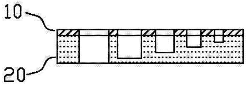
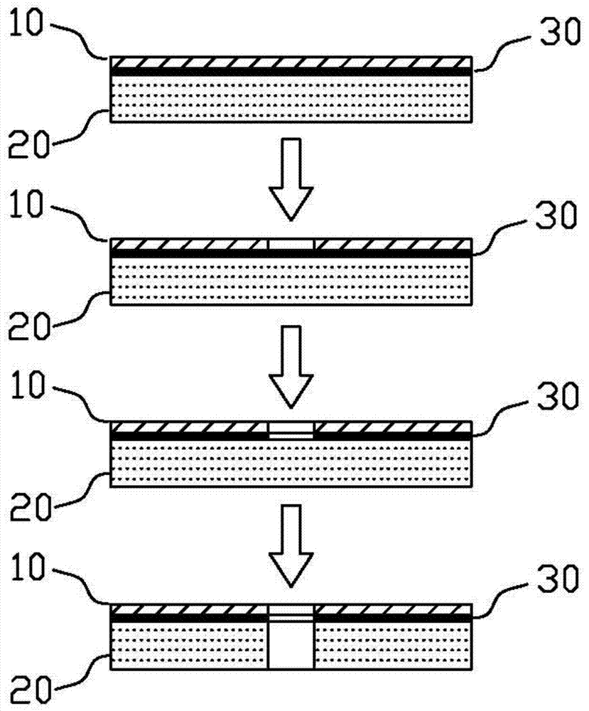
[0031] The present invention mainly proposes a method for preparing an ultra-high-precision silicon-based through-hole pattern structure, which includes the following steps:

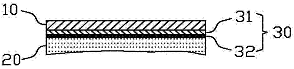
[0032] Fabricate an inorganic mask layer on the silicon substrate;

[0033] Coating photoresist on the inorganic mask layer, and etching to form a photoresist pattern structure;

[0034] Etching the inorganic mask layer by using the photoresist pattern structure as a mask;

[0035] Using the etched inorganic mask layer as a mask, a dry etching process is used to etch the silicon substrate to form a pattern structure of through holes on the silicon substrate.

[0036] Further, in the dry etching process, for openings with a diameter of less than 2 μm, the silicon etching selectivity ratio of the inorganic mask layer at room temperature is above 1:1000, and the silicon substrate Before the etching depth of the area corresponding to the minimum aperture in the through-hole pattern structure reaches a set ...


PUM

PropertyMeasurementUnit
thicknessaaaaaaaaaa
thicknessaaaaaaaaaa

Abstract

A method for preparing an ultra-high-precision silicon-based through-hole pattern structure, comprising: making an inorganic mask layer on a silicon substrate; coating photoresist on the inorganic mask layer, and etching to form a photoresist pattern structure; Etching the inorganic mask layer with the photoresist pattern structure as a mask; using the etched inorganic mask layer as a mask, using a dry etching process to etch the silicon substrate to form through holes on the silicon substrate pattern structure, and in the dry etching process, for openings with a diameter below 2 μm, the silicon etching selectivity ratio of the inorganic mask layer at room temperature is above 1:1000, and the silicon substrate and the The inorganic mask layer is not completely removed by etching before the etching depth of the corresponding area at the smallest aperture in the via hole pattern structure reaches a set depth. The preparation method of the invention has simple process and low cost, and can realize efficient and fast large-scale preparation with high-precision submicron silicon-based through-hole patterns, thereby fully meeting the requirements of practical applications.

Description

technical field [0001] The invention relates to a deep silicon etching process, in particular to a method for preparing a submicron ultra-high-precision silicon-based through-hole pattern structure by using deep silicon etching, and belongs to the technical field of semiconductor manufacturing. Background technique [0002] Deep silicon etching is a technology for etching single crystal silicon materials commonly used in semiconductor device manufacturing, micro-electro-mechanical systems (Micro-Electro-Mechanical Systems, MEMS), 3D packaging and other fields. This technology can be applied in various research and production fields such as hollow mask, MEMS sensor, porous silicon fabrication, chip manufacturing and so on. [0003] The typical deep silicon etching technology is to etch single crystal silicon by alternating ion etching-deposition steps. This etching method is also called Bosch etching method. The mask layer used is generally photoresist (PR ) or SiO 2 layer,...

Claims


Application Information

Patent Timeline
Patent Type & Authority Patents(China)
IPC IPC(8): H01L21/768
Inventor 包文中
Owner 浙江赛威科光电科技有限公司
Why Eureka
Try Eureka