Growth method for GaN-based LED epitaxial wafer
A technology of LED epitaxial wafer and growth method, applied in the direction of crystal growth, single crystal growth, single crystal growth, etc., can solve the problems of unfavorable crystal quality and epitaxial surface, complex process technology, increased forward voltage, etc.
- Summary
- Abstract
- Description
- Claims
- Application Information
AI Technical Summary
Problems solved by technology
Method used
Image

Examples
Embodiment 1
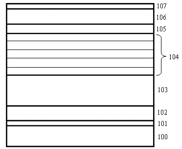
[0034] The MOCVD method is used to grow sequentially from bottom to top:
[0035] 1. Put the sapphire substrate with (0001) crystal orientation into the reaction chamber, and then 2 Heating to 1100° C. under atmosphere and baking for 8 minutes to purify the substrate at high temperature.
[0036] 2. Lower the temperature to 530°C to grow a low-temperature GaN buffer layer with a thickness of 30nm.
[0037] 3. A non-doped GaN layer with a thickness of 2 microns was grown at 1070°C.
[0038] 4. Grow an n-type GaN layer with a thickness of 2 microns at 1070°C.
[0039] 5. Grow 10 cycles of InGaN / GaN multi-quantum well layers, the thickness of the GaN barrier layer is 22nm, the growth temperature is 860°C; the thickness of the InGaN well layer is 3nm, the growth temperature is 740°C, and the growth time is 5 minutes. During the whole growth process of the InGaN well layer for 5 minutes, hydrogen gas is completely injected, and the flow rate is 0.01 slm.
[0040] 6. Raise the t...
Embodiment 2
[0047] The growth conditions of other steps are the same as in Example 1.
[0048] The difference is that in step 5, the InGaN / GaN multi-quantum well layer is grown for 15 cycles, the thickness of the GaN barrier layer is 20nm, and the growth temperature is 860°C; the thickness of the InGaN well layer is 2.5nm, the growth temperature is 740°C, and the growth time for 3 minutes. 1 minute after the start of the growth of the InGaN well layer, hydrogen gas was introduced, the flow rate was 10 slm, and the duration was 0.1 minute.
[0049] The epitaxial wafer obtained in this embodiment was fabricated into a 300 micron×300 micron chip using ITO as a transparent electrode according to a standard chip process. After the test, the brightness has increased by 25% compared with the normal process, the reverse voltage has increased by 12V, and the forward voltage has decreased by 0.15V.
Embodiment 3
[0051] The growth conditions of other steps are the same as in Example 1.
[0052] The difference is that in step 5, 20 cycles of InGaN / GaN multi-quantum well layers are grown, the thickness of the GaN barrier layer is 18nm, and the growth temperature is 860°C; the thickness of the InGaN well layer is 2nm, the growth temperature is 740°C, and the growth time is 2.5 minutes. 0.2 minutes after the start of the growth of the InGaN well layer, hydrogen gas was introduced, the flow rate was 0.2 slm, and the duration was 2.3 minutes.
[0053] The epitaxial wafer obtained in this embodiment was fabricated into a 300 micron×300 micron chip using ITO as a transparent electrode according to a standard chip process. After the test, the brightness increased by 20% compared with the normal process, the reverse voltage increased by 8V, and the forward voltage decreased by 0.08V.
PUM
| Property | Measurement | Unit |
|---|---|---|
| thickness | aaaaa | aaaaa |
| thickness | aaaaa | aaaaa |
Abstract
Description
Claims
Application Information
 - R&D
- Intellectual Property
- Life Sciences
- Materials
- Tech Scout
- Unparalleled Data Quality
- Higher Quality Content
- 60% Fewer Hallucinations
Browse by: Latest US Patents, China's latest patents, Technical Efficacy Thesaurus, Application Domain, Technology Topic, Popular Technical Reports.
© 2025 PatSnap. All rights reserved.Legal|Privacy policy|Modern Slavery Act Transparency Statement|Sitemap|About US| Contact US: help@patsnap.com