


Quick Research
Generate reliable direction feasibility study reports for your R&D in just a few steps.

Technical Q&A
Discover and master advanced knowledge NOW. Basics, ideas, possibilities, all at once.

Find Solutions
As an expert in R&D theories, this can generate solutions to your technical problems instantly.

Evaluate Feasibility
Analyze your overall solution with one click, know your potential R&D risks in advance.

Monitor Landscape
Get weekly tech updates, stay abreast of the latest tech innovations and key insights.
LED epitaxial growth method for enhancing antistatic effect of device
An epitaxial growth, anti-static technology, applied in semiconductor devices, semiconductor/solid-state device manufacturing, circuits, etc., can solve the problems of weak anti-static ability, weakened anti-static ability, and poor crystal quality of LED devices, and achieve low dislocation density. , The effect of improving antistatic ability and improving crystal quality
- Summary
- Abstract
- Description
- Claims
- Application Information
AI Technical Summary
Problems solved by technology
Method used
Image

Examples
Embodiment 1
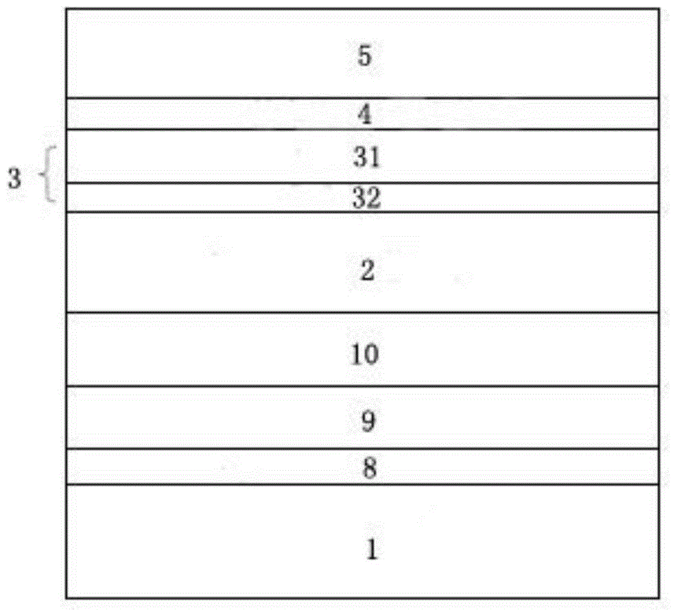
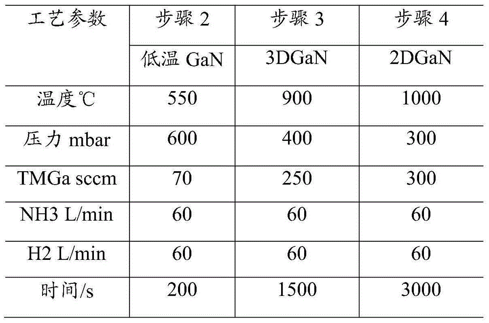
[0023] The invention uses MOCVD to grow high-brightness GaN-based LED epitaxial wafers. Use high-purity H2 or high-purity N2 or a mixture of high-purity H2 and high-purity N2 as the carrier gas, high-purity NH3 as the N source, metal organic source trimethylgallium (TMGa) as the gallium source, trimethylindium (TMIn ) as the indium source, the N-type dopant as silane (SiH4), trimethylaluminum (TMAl) as the aluminum source, the P-type dopant as magnesocene (CP2Mg), and the substrate as (0001) sapphire, the reaction The pressure is between 100mbar and 800mbar.
[0024] Step 101: maintaining the temperature at 900° C., maintaining the pressure in the reaction chamber at 100 mbar, and injecting 50 L / min of hydrogen gas to treat the sapphire substrate 1 at high temperature for 5 minutes;
[0025] Step 102: Maintaining the temperature at 700°C and maintaining the pressure in the reaction chamber at 100mbar, injecting 50L / min of hydrogen gas, 50L / min of ammonia gas, and 100 sccm of ...
Embodiment 2
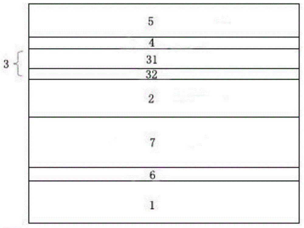
[0033] Step 201: maintaining the temperature at 1100° C., maintaining the pressure in the reaction chamber at 200 mbar, and injecting 100 L / min of hydrogen to treat the sapphire substrate 1 at high temperature for 10 minutes;
[0034] Step 202: maintaining the temperature at 800° C. and the pressure of the reaction chamber at 300 mbar, feeding 100 L / min of hydrogen gas, 100 L / min of ammonia gas, and 200 sccm of TMAl source to grow an AlN layer 6 with a thickness of 60 nm on the sapphire substrate;
[0035] Step 203: Raise the temperature to 900° C., maintain the pressure of the reaction chamber at 300 mbar, feed 100 L / min of hydrogen gas, 100 L / min of ammonia gas, 300 sccm of TMGa source, and 200 sccm of TMAl to continuously grow 5 μm of Al on the AlN layer 6 x Ga ( 1-x) N layer 7, the value range of x is between 0-1, which is 0.8 in this embodiment;
[0036] Step 204: Keep the temperature at 1100°C, maintain the pressure in the reaction chamber at 300mbar, feed 90L / min of hy...
Embodiment 3
[0042] Step 301: maintaining the temperature at 1000° C., maintaining the pressure in the reaction chamber at 150 mbar, and injecting 75 L / min of hydrogen gas to treat the sapphire substrate 1 at high temperature for 7 minutes;
[0043] Step 302: maintaining the temperature at 750° C. and the pressure of the reaction chamber at 200 mbar, feeding 75 L / min of hydrogen gas, 75 L / min of ammonia gas, and 150 sccm of TMAl source to grow an AlN layer 6 with a thickness of 40 nm on the sapphire substrate;
[0044] Step 303: Raise the temperature to 850° C., maintain the pressure of the reaction chamber at 200 mbar, feed 75 L / min of hydrogen gas, 75 L / min of ammonia gas, 250 sccm of TMGa source, and 125 sccm of TMAl to continuously grow 4 μm of Al on the AlN layer 6 x Ga (1-x) N layer 7, the value of x is 0.5;
[0045] Step 304: Keep the temperature at 1050°C, maintain the pressure in the reaction chamber at 225mbar, feed 70L / min of hydrogen, 50L / min of ammonia, 250sccm of TMGa source...
PUM
 Abstract
Description
Claims
Application Information
 - R&D Engineer
- R&D Manager
- IP Professional
- Industry Leading Data Capabilities
- Powerful AI technology
- Patent DNA Extraction
Browse by: Latest US Patents, China's latest patents, Technical Efficacy Thesaurus, Application Domain, Technology Topic, Popular Technical Reports.
© 2024 PatSnap. All rights reserved.Legal|Privacy policy|Modern Slavery Act Transparency Statement|Sitemap|About US| Contact US: help@patsnap.com