Method for preparing P-type low-defect silicon carbide epitaxial wafer
A silicon carbide and epitaxial wafer technology, which is applied to electrical components, circuits, semiconductor devices, etc., can solve the problems of long consumption time, limited effect of ultra-thick silicon carbide epitaxial wafers, and reduced quality of epitaxial layers, etc. The effect of period extension and reduction of basal plane dislocation density
- Summary
- Abstract
- Description
- Claims
- Application Information
AI Technical Summary
Problems solved by technology
Method used
Image
Examples
Embodiment 1
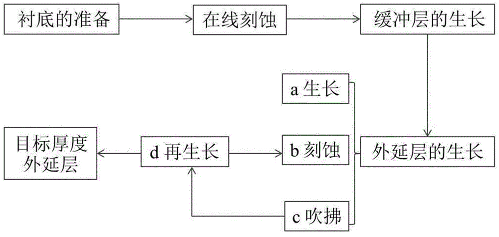
[0033] A method for preparing a P-type low-defect thickness 15um silicon carbide epitaxial wafer, comprising the following steps:
[0034] 1) Etching the substrate online: place a 4H-SiC substrate in the reaction chamber, vacuumize, and feed in hydrogen gas at a flow rate of 40L / min and HCl at a flow rate of 5L / min. The pressure in the reaction chamber is 40mbar and the temperature is 1680°C. minute;
[0035] 2) Growth of the buffer layer: Stop feeding HCl, lower the temperature to 1650°C, and feed SiH with a flow rate of 6mL / min 4 and 3mL / min of C 3 h 8 , using trimethylaluminum TMA with a flow rate of 1500mL / min as a dopant, and a growth pressure of 40mbar;
[0036] 3) Growth of epitaxial layer
[0037] a Growth: 40L / min flow rate of hydrogen, 10mL / min SiH 4 and 5mL / min of C 3 h 8 Pass it into the reaction chamber, keep the temperature at 1650°C and the pressure at 40mbar, and use trimethylaluminum TMA at a flow rate of 800mL / min as the dopant to grow an epitaxial lay...
Embodiment 2
[0042] A method for preparing a P-type low-defect thickness 30um silicon carbide epitaxial wafer, comprising the following steps:
[0043] 1) Etching the substrate online: place a 4H-SiC substrate in the reaction chamber, vacuumize, and feed in hydrogen gas at a flow rate of 40L / min and HCl at a flow rate of 5L / min. The pressure in the reaction chamber is 40mbar and the temperature is 1680°C. minute;
[0044] 2) Growth of the buffer layer: Stop feeding HCl, lower the temperature to 1650°C, and feed SiH with a flow rate of 6mL / min 4 and 3mL / min of C 3 h 8 , using trimethylaluminum TMA with a flow rate of 1500mL / min as a dopant, and a growth pressure of 40mbar;
[0045] 3) Growth of epitaxial layer
[0046] a Growth: 40L / min flow rate of hydrogen, 10mL / min SiH 4 and 5mL / min of C 3 h 8 Pass it into the reaction chamber, keep the temperature at 1650°C and the pressure at 40mbar, and use trimethylaluminum TMA at a flow rate of 800mL / min as the dopant to grow an epitaxial lay...
Embodiment 3
[0054] A method for preparing a P-type low-defect silicon carbide epitaxial wafer with a thickness of 80um, comprising the following steps:
[0055] 1) Etching the substrate online: place a 4H-SiC substrate in the reaction chamber, vacuumize, and feed in hydrogen gas at a flow rate of 40L / min and HCl at a flow rate of 5L / min. The pressure in the reaction chamber is 40mbar and the temperature is 1680°C. minute;
[0056] 2) Growth of the buffer layer: Stop feeding HCl, lower the temperature to 1650°C, and feed SiH with a flow rate of 6mL / min 4 and 3mL / min of C 3 h 8 , using trimethylaluminum TMA with a flow rate of 1500mL / min as a dopant, and a growth pressure of 40mbar;
[0057] 3) Growth of epitaxial layer
[0058] a Growth: 40L / min flow rate of hydrogen, 10mL / min SiH 4 and 5mL / min of C 3 h 8 Pass it into the reaction chamber, keep the temperature at 1650°C and the pressure at 40mbar, and use trimethylaluminum TMA at a flow rate of 800mL / min as the dopant to grow an epi...
PUM
| Property | Measurement | Unit |
|---|---|---|
| thickness | aaaaa | aaaaa |
| thickness | aaaaa | aaaaa |
| thickness | aaaaa | aaaaa |
Abstract
Description
Claims
Application Information
 - R&D
- Intellectual Property
- Life Sciences
- Materials
- Tech Scout
- Unparalleled Data Quality
- Higher Quality Content
- 60% Fewer Hallucinations
Browse by: Latest US Patents, China's latest patents, Technical Efficacy Thesaurus, Application Domain, Technology Topic, Popular Technical Reports.
© 2025 PatSnap. All rights reserved.Legal|Privacy policy|Modern Slavery Act Transparency Statement|Sitemap|About US| Contact US: help@patsnap.com


