Focusing plane positioning device and method of laser micro-beam back irradiation chip test
A technology of focusing plane and positioning device, which is applied in the field of laser micro-beam irradiation test, and can solve the problems that cannot meet the needs of positioning
- Summary
- Abstract
- Description
- Claims
- Application Information
AI Technical Summary
Problems solved by technology
Method used
Image
Examples
Embodiment 1
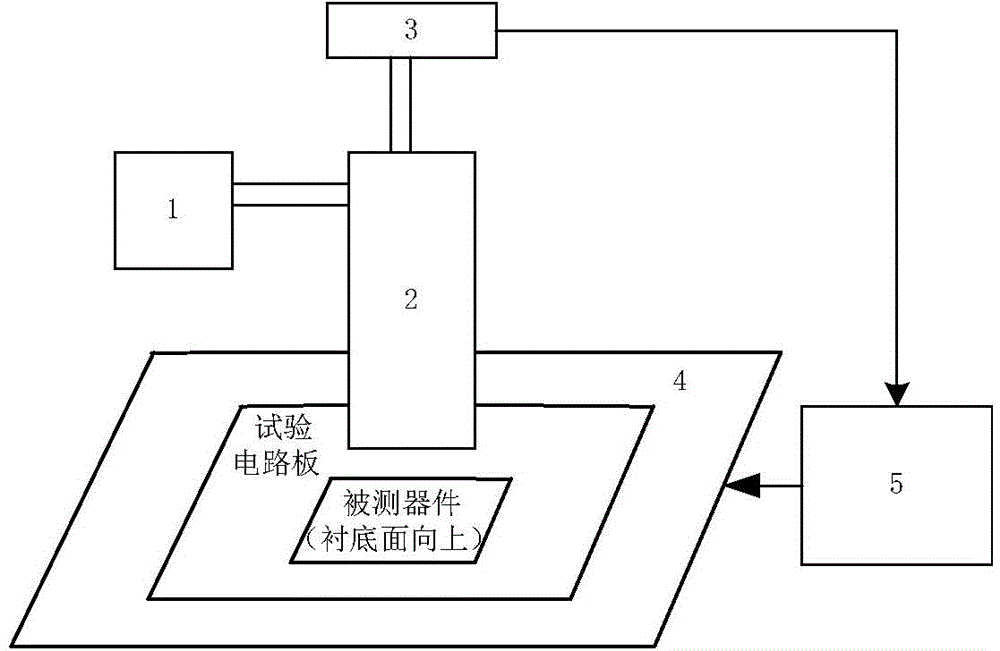
[0065] Such as figure 1 As shown, the focal plane positioning device for the laser microbeam back irradiation chip test is used for positioning the focal plane of the device under test. The device includes a laser source 1 for testing, a focusing optical path adjustment module 2, an imaging CCD module 3, a The mobile station 4 and the three-dimensional mobile station control module 5 .
[0066] The test laser source 1 is used to emit pulsed laser with fixed parameters;
[0067] The focusing optical path adjustment module 2 is used to adjust the pulsed laser emitted by the test laser source 1 to make it a test laser beam;
[0068] The imaging CCD module 3 is used to image the laser reflection spot of the device under test, and output the reflection spot imaging signal to the three-dimensional mobile station control module 5;
[0069] The three-dimensional mobile station 4 is used to place the test circuit board of the device under test;
[0070] The three-dimensional mobile ...
Embodiment 2
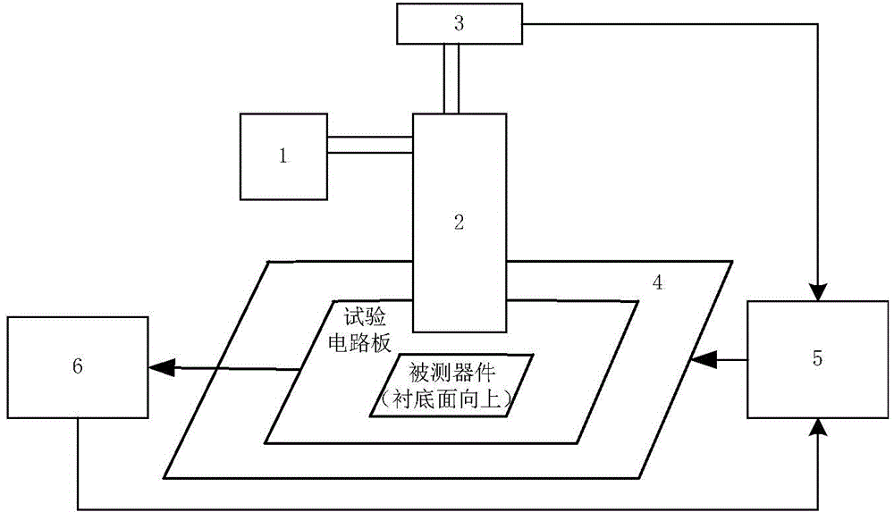
[0074] Based on the device in Example 1, in Example 2, such as figure 2 As shown, the device further includes: a device electrical feature acquisition analysis processing module 6, and the three-dimensional mobile station control module 5 also includes an electrical feature processing unit and a second control unit;
[0075] The device electrical characteristic acquisition analysis processing module 6 is used to receive the signal output by the test circuit board of the device under test, and output the processed signal to the electrical characteristic processing unit;
[0076] The electrical characteristic processing unit is used to receive the signal output by the device electrical characteristic acquisition analysis processing module 6, perform statistical analysis and processing, form a feedback signal instruction, and output it to the second control unit;
[0077] The second control unit is used to receive the feedback signal instruction sent by the electrical characteri...
Embodiment 3
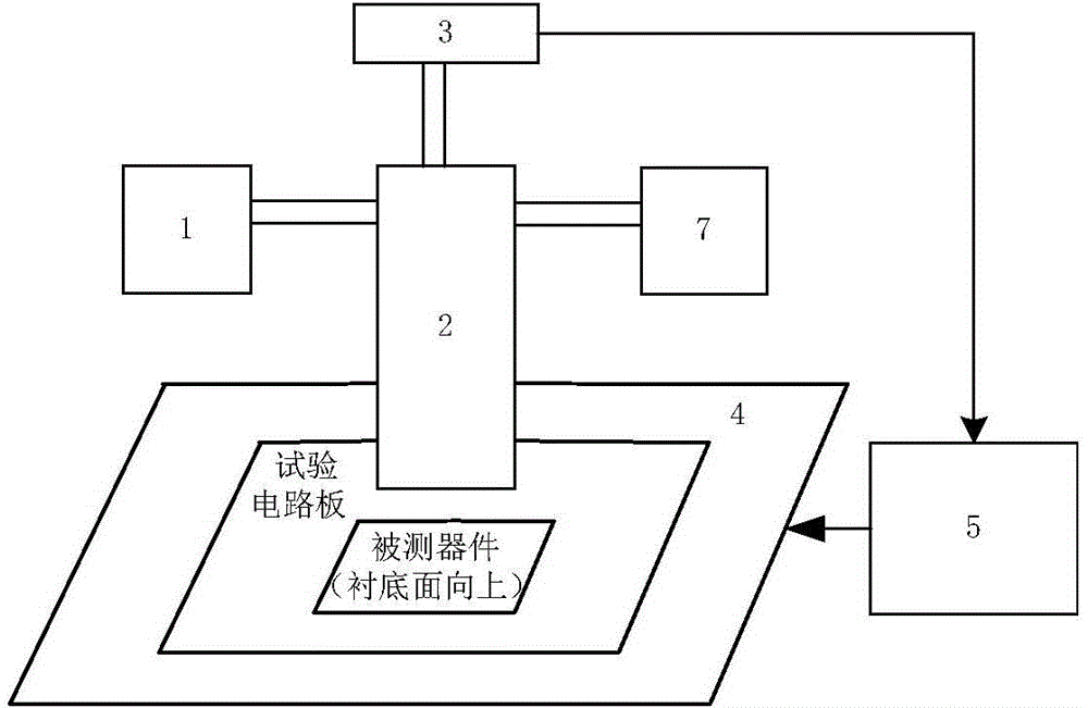
[0079] Based on the device in Example 1, in Example 3, such as image 3 As shown, the device further includes: a light source 7 for illumination, and the three-dimensional mobile station control module 5 also includes a second CCD imaging processing unit and a third control unit;
[0080]The illumination light source 7 is used to emit illumination light onto the device under test, and the CCD imaging module 3 will image the metal reflective layer of the device under test; and output the imaging signal to the second CCD for imaging processing unit; the second CCD imaging processing unit outputs a feedback signal instruction to the third control unit according to the definition of imaging;
[0081] The second CCD imaging processing unit is used to receive the imaging signal output by the imaging CCD module 3, and form a feedback signal instruction after performing imaging definition detection, and output it to the third control unit;
[0082] The third control unit is configure...
PUM
 Abstract
Description
Claims
Application Information
 - R&D
- Intellectual Property
- Life Sciences
- Materials
- Tech Scout
- Unparalleled Data Quality
- Higher Quality Content
- 60% Fewer Hallucinations
Browse by: Latest US Patents, China's latest patents, Technical Efficacy Thesaurus, Application Domain, Technology Topic, Popular Technical Reports.
© 2025 PatSnap. All rights reserved.Legal|Privacy policy|Modern Slavery Act Transparency Statement|Sitemap|About US| Contact US: help@patsnap.com


