Substrate for inversely installed LED chip and manufacturing method thereof

A technology of LED chip and manufacturing method, which is applied in the direction of electrical components, circuits, semiconductor devices, etc., can solve the problems that the quantum efficiency in the LED chip cannot be fully exerted, destroy the light output effect of the flip-chip LED chip, and reduce the light output efficiency, etc., so as to avoid Lithographic alignment is difficult, suitable for large-scale commercial production, and the effect of improving internal quantum efficiency

Active Publication Date: 2015-09-02
HANGZHOU SILAN AZURE
View PDF5 Cites 2 Cited by
  • Summary
  • Abstract
  • Description
  • Claims
  • Application Information

AI Technical Summary

Problems solved by technology

However, the flip-chip LED chip structure emits light on the N side. Since the refractive index of sapphire is lower than that of gallium nitride, the light emitted from the epitaxial layer will be reflected on the interface between the sapphire and the substrate, resulting in more light. It cannot be emitted, especially the patterned substrate currently used in the mainstream of the LED chip structure has scattering and diffuse reflection effects, which is more likely to cause more light not to be emitted, reducing the light extraction efficiency
Not only that, after the patterned substrate replaces the flat substrate, the surface of the patterned substrate must be filled with a thicker buffer layer to ensure that the epitaxial layer on the substrate has a higher crystal quality. However, the buffer The layer is generally a polycrystalline material, which has a high light absorption rate, which seriously damages the light-emitting effect of the flip-chip LED chip; however, if the patterned substrate technology is not used, the internal quantum efficiency of the LED chip cannot be fully utilized.

Method used


Image

  • Substrate for inversely installed LED chip and manufacturing method thereof
  • Substrate for inversely installed LED chip and manufacturing method thereof
  • Substrate for inversely installed LED chip and manufacturing method thereof

Examples


Embodiment 1

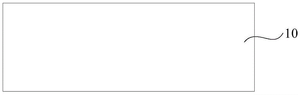
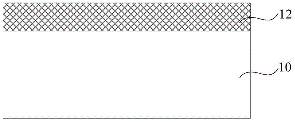
[0067] Figure 10 It is a top view of a substrate for flip-chip LED chips according to Embodiment 1 of the present invention, Figure 9 yes Figure 10 Schematic cross-sectional view of the structure shown along the direction AA'. Such as Figure 9-10 As shown, the substrate for a flip-chip LED chip includes: a support substrate 10, a lattice matching layer 11 having the same crystal structure as the epitaxial layer of the flip-chip LED chip, and a dielectric layer 12, wherein the dielectric layer 12 is a columnar structure arranged in an array, the lattice matching layer 11 is formed on the support substrate 10 , and the columnar structure is embedded in the lattice matching layer 11 .

[0068] Wherein, the columnar structure may be a columnar structure, an elliptical columnar structure, or a polygonal columnar structure. In this embodiment, the columnar structure is a hexagonal columnar structure. Of course, since the supporting substrate 10 is a circular substrate, the ...

Embodiment 2

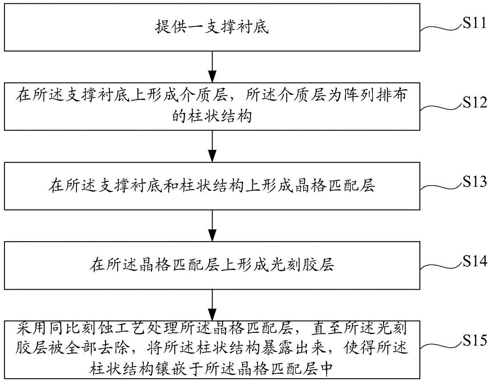
[0090] The structure of the substrate for flip-chip LED chips in this embodiment is the same as that of Embodiment 1, but the manufacturing method adopted in this embodiment is different, such as Figure 11 As shown, the manufacturing method for the substrate of the flip-chip LED chip provided by the present invention comprises the following steps:

[0091] S21: providing a supporting substrate;

[0092] S22: forming a lattice matching layer on the support substrate, the lattice matching layer having columnar holes arranged in an array;

[0093] S23: forming a dielectric layer on the support substrate and the lattice matching layer;

[0094] S24: forming a photoresist layer on the dielectric layer;

[0095] S25: performing a backlighting and developing process on the support substrate, and removing the photoresist layer directly above the lattice matching layer;

[0096] S26: Etching and removing the dielectric layer directly above the lattice matching layer to form a colum...

Embodiment 3

[0109] The difference between the substrate for flip-chip LED chips in this embodiment and the first embodiment is that the lattice matching layer 11 is a columnar structure, and the dielectric layer 12 is formed on the supporting substrate 10, so The dielectric layer 12 has columnar holes arranged in an array, and the lattice matching layer 11 is embedded in the dielectric layer 10 through the columnar holes.

[0110] Figure 30 It is a top view of a substrate for flip-chip LED chips according to Embodiment 3 of the present invention, Figure 29 yes Figure 30 Schematic cross-sectional view of the structure shown along the direction AA'. Such as Figures 29-30 As shown, the substrate for the flip-chip LED chip includes: a support substrate 10, a lattice matching layer 11 having the same crystal structure as the epitaxial layer of the flip-chip LED chip, and a dielectric layer 12, wherein the lattice The matching layer 11 is a columnar structure arranged in an array, and t...


PUM


Abstract

The invention provides a substrate for an inversely installed LED chip and a manufacturing method thereof. The substrate includes a support substrate, a dielectric layer, and a crystal lattice matching layer in the same structure with an epitaxial layer crystal structure of the inversely installed LED chip, the dielectric layer and the crystal lattice matching layer are arranged on the support substrate, the crystal lattice matching layer is in a cylinder structure arranged in an array and is embedded in the dielectric layer, or, the dielectric layer is in a cylinder structure arranged in an array and is embedded in the crystal lattice matching layer. The crystal quality of the inversely installed LED chip is improved, namely, the internal quantum efficiency is improved, the reflection of light from the epitaxial layer to the substrate can be reduced, the transmission is increased, the luminous efficiency of the inversely installed LED chip is improved, namely, the external quantum efficiency is improved.

Description

technical field [0001] The invention belongs to the field of manufacturing semiconductor optoelectronic chips, in particular to a substrate for flip-chip LED chips and a manufacturing method thereof. Background technique [0002] Since the commercialization of GaN-based LEDs in the early 1990s, after more than 20 years of development, its structure has become mature and perfect, and it has been able to meet people's current needs for lighting decoration; but it must completely replace traditional light sources and enter the lighting industry. In the field of lighting, especially in the field of high-end lighting, the improvement of luminous brightness is the never-ending pursuit of scientific researchers in the LED industry. In recent years, the most active technology in improving LED luminance is undoubtedly the patterned substrate technology. The patterned substrate technology not only improves the crystal quality of LED epitaxy by reducing lattice defects (or lattice mism...

Claims


Application Information

Patent Timeline
Patent Type & Authority Applications(China)
IPC IPC(8): H01L33/22H01L33/00
CPCH01L33/005H01L33/22
Inventor 马新刚丁海生李东昇陈善麟江忠永
Owner HANGZHOU SILAN AZURE
Why Eureka
Try Eureka