Clock network traversing testing method based on FPGA (Field Programmable Gate Array) hardware structure

A clock network and traversal test technology, applied in the field of integrated circuits, can solve the problems of increasing test time, test cost, scarcity of resources, etc., and achieve the effect of reducing the number of configurations, reducing the number of configurations, and improving portability

Active Publication Date: 2015-05-13
FUDAN UNIV
View PDF5 Cites 14 Cited by
  • Summary
  • Abstract
  • Description
  • Claims
  • Application Information

AI Technical Summary

Problems solved by technology

The obvious disadvantage of this method is that because the IO (input and output) ports of the FPGA are much rarer than the internal resources of the

Method used


Image

  • Clock network traversing testing method based on FPGA (Field Programmable Gate Array) hardware structure
  • Clock network traversing testing method based on FPGA (Field Programmable Gate Array) hardware structure
  • Clock network traversing testing method based on FPGA (Field Programmable Gate Array) hardware structure

Examples


Embodiment Construction

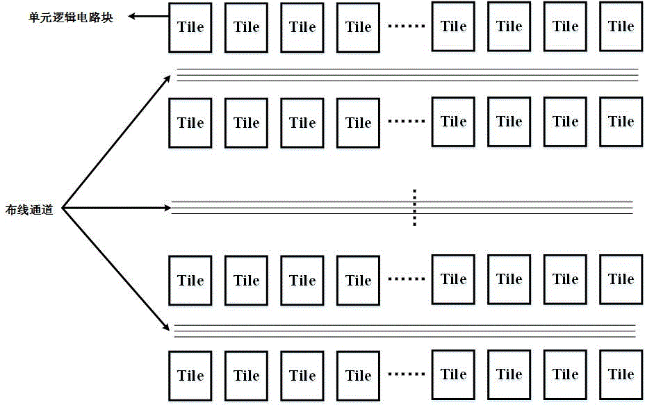
[0024] For the unit circuit whose basic logic block is CLB, all SLICEs are Figure 5 configured as shown. Configure the output of all SLICEs to operate in clock edge-based modes, such as flip-flops. In this mode of operation, short circuit, open circuit, normal 0 and normal 1 faults of the clock signal can be detected. Configure one SLICE in a logic unit as a four-input AND operation unit, and configure the other three as a state where the output is always 1 after the clock signal arrives, and connect it to the three input terminals of the first SLICE, and the other three of the SLICE One input comes from the output of the upper logic unit. After all the CLBs in the FPGA are configured in this way, the entire FPGA is like a shift chain. If all clock terminals can work normally, then after N clock cycles, the input value will be shifted out. Among them, N is the number of all CLB logic blocks in the FPGA. If any clock input terminal in the chip fails, for example, the cloc...


PUM


Abstract

The invention belongs to the technical field of testing of integrated circuits, and specially provides a clock network traversing testing method based on the FGPA (Field Programmable Gate Array). The method is that each logic block is configured as that the SLICE in the a CLB logic block circuit (Configurable Logic Block) is configured to be in a logic gate operation form; a BRAM logic block circuit is configured to the read-only ROM address searching mode; a DSP logic block circuit is configured to be in some operation form; all configuration modes above are under the control of a clock signal, and the result is outputted through a register; the faults which can be tested include short circuit, open circuit, general 0 and 1 faults of an FPGA clock end. With the adoption of the method, the clock input ends of all unit block circuits in an FPGA chip and all clock network functions can be tested; the configuration times, configuration difficulty and the testing time for testing are greatly optimized.

Description

technical field [0001] The invention belongs to the technical field of integrated circuits, and in particular relates to a traversal test method for a clock network in an FPGA (Field Programmable Gate Array). Background technique [0002] As a semi-customized integrated circuit, FPGA not only solves the problems of long ASIC design cycle, high manufacturing cost and complex production process, but also avoids the shortcomings of the original programmable logic device gates with limited number and low operating frequency. . FPGA can be programmed through the hardware description language Verilog HDL or VHDL, the user uses the hardware description language to design the circuit, and then compiles and generates the bit stream file through the corresponding FPGA development software and downloads it to the FPGA chip, so that the FPGA chip can be quickly configured into the designed circuit. [0003] With the continuous expansion of FPGA chip scale and application fields, the t...

Claims


Application Information

Patent Timeline
IPC IPC(8): H03K5/135G06F11/22
Inventor 杨震王健来金梅
Owner FUDAN UNIV
Why Eureka
Try Eureka