Semiconductor device
A semiconductor and substrate technology, applied in semiconductor devices, semiconductor/solid-state device manufacturing, electric solid-state devices, etc., can solve the problems of process flow difficulties, inability to fully utilize SiC features, and reduced mechanical strength of SiC chips, and achieve reliable welding. Effect
- Summary
- Abstract
- Description
- Claims
- Application Information
AI Technical Summary
Problems solved by technology
Method used
Image
Examples
Embodiment 1
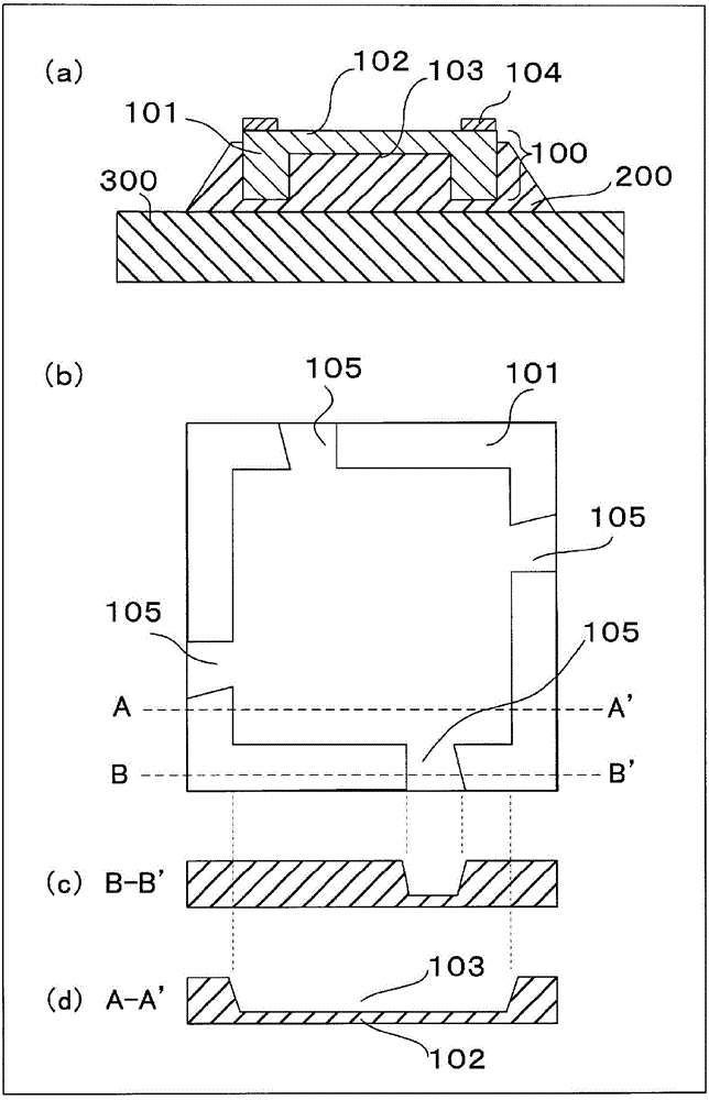
[0053] figure 1 It is an explanatory diagram showing the structure of the semiconductor device according to Embodiment 1 of the present invention. figure 1 (a) is a sectional view, figure 1 (b) is a plan view when viewing a semiconductor chip from the back surface. in addition, figure 1 (c) is figure 1 Section view on line B-B' of (b), figure 1 (d) is figure 1 Sectional view on line A-A' of (b). In Example 1, a SiC substrate (semiconductor chip) 100 in which an SiC epitaxial layer was formed on a bulk substrate (hereinafter referred to as bulk SiC) made of silicon carbide (SiC) was used, and the surface on the side of the SiC epitaxial layer was used as a chip. Surface The surface element structure 102 of MOSFET is formed on the surface of the chip. Bulk SiC and SiC epitaxial layers are n-type.
[0054] Specifically, on the SiC epitaxial layer on the surface side of the semiconductor chip 100, a MOS gate (insulated gate composed of a metal-oxide film-semiconduct...
Embodiment 2
[0080] Example 2 is an example in which the groove shape of the rib on the back surface of the chip is changed from Example 1. Figure 7 It is an explanatory diagram showing the structure of a semiconductor device according to Embodiment 2 of the present invention. Figure 7 (a) is a plan view when viewing a semiconductor chip from the back surface. in addition, Figure 7 (b) is Figure 7 Section view on line B-B' of (a), Figure 7 (c) is Figure 7 Sectional view on line A-A' of (a). In Embodiment 2, as the shape of the groove 105 for suppressing the rotation of the semiconductor chip, the side wall of the groove 105 on the side away from the corner of the rib 101 is inclined relative to the other side wall so that the rib 101 The inner peripheral side increases the width of the groove 105 toward the side away from the corner of the rib 101 , and the width of the groove 105 becomes smaller from the inner side toward the outer side. In the chip mounted on the solder pellets...
Embodiment 3
[0082] Example 3 is an example in which the planar shape of the concave portion on the back surface of the chip is changed from Example 1. Figure 8 It is an explanatory diagram showing the structure of a semiconductor device according to Embodiment 3 of the present invention. Figure 8 (a) is a plan view when viewing a semiconductor chip from the back surface, Figure 8 (b) is Figure 8 Sectional view on line A-A' of (a). In Example 3, the planar shape of the concave portion 103 on the back surface of the chip is circular so that voids are less likely to be generated inside the concave portion 103 . In this example, measures to suppress the rotation of the semiconductor chip are not given to the groove 105 , but the shape of the groove 105 may be changed as in the first and second embodiments to take measures to suppress the rotation of the semiconductor chip.
PUM
 Abstract
Description
Claims
Application Information
 - R&D
- Intellectual Property
- Life Sciences
- Materials
- Tech Scout
- Unparalleled Data Quality
- Higher Quality Content
- 60% Fewer Hallucinations
Browse by: Latest US Patents, China's latest patents, Technical Efficacy Thesaurus, Application Domain, Technology Topic, Popular Technical Reports.
© 2025 PatSnap. All rights reserved.Legal|Privacy policy|Modern Slavery Act Transparency Statement|Sitemap|About US| Contact US: help@patsnap.com


