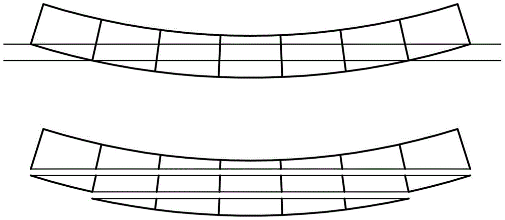
A method for homoepitaxial growth on gan substrate
A homoepitaxial and epitaxial growth technology, which is applied in semiconductor/solid-state device testing/measurement, coating, gaseous chemical plating, etc. Quantum recombination efficiency, external quantum emission efficiency, and effect of reducing dislocation density
- Summary
- Abstract
- Description
- Claims
- Application Information
AI Technical Summary
Problems solved by technology
Method used
Image
Examples
Embodiment 1
[0036] Example 1: Homoepitaxial growth on c-plane self-supporting GaN substrate
[0037] Include the following steps:
[0038] 1) The GaN substrate is grown by HVPE method. After cleaning, the radius of curvature of the surface is measured. In this embodiment, the thickness of the sample is 2000 μm, and the radius of curvature is 10 meters.
[0039] 2) A relatively flat GaN substrate is obtained by chemical mechanical polishing (CMP), and a silicon dioxide mask layer with a thickness of 100 nm is deposited by PECVD.
[0040] 3) Concentric mask rings with a width of 1-20 μm are formed by using a conventional semiconductor photolithography process; the pitch of the concentric rings is 1-100 μm.
[0041] 4) After cleaning, put it into MOCVD for growth. The growth process uses nitrogen, hydrogen or a mixture of the two as the carrier gas. The temperature of the epitaxial GaN layer is 900°C-1200°C, and the pressure is 100-500Torr. In this embodiment, the obtained GaN epitaxial la...
Embodiment 2
[0043] Embodiment two: the growth based on the light-emitting diode (LED) of embodiment one
[0044] A conventional semiconductor photolithography process is used to form concentric mask rings with a width of 1 μm, and the pitch of the concentric rings is 1 μm. After cleaning, it is placed in MOCVD for growth. The growth process uses nitrogen and hydrogen as carrier gases. The temperature of the epitaxial GaN layer is 900°C-1200°C, the pressure is 100-500Torr, and the thickness of the growth surface is 5μm. Use the 5μm thick GaN epitaxial wafer grown by MOCVD as the substrate, and continue to grow light-emitting diodes (LEDs) by MOCVD. Due to the modulated growth of the annular mask, a light-emitting diode with an increase in light extraction efficiency of more than 50% can be obtained .
Embodiment 3
[0045] Embodiment three: the growth based on the light-emitting diode (LED) of embodiment one
[0046] A conventional semiconductor photolithography process is used to form concentric mask rings with a width of 1 μm and a pitch of 100 μm. After cleaning, it is placed in MOCVD for growth. The growth process uses nitrogen and hydrogen as carrier gases. The temperature of the epitaxial GaN layer is 900°C-1200°C, the pressure is 100-500Torr, and the thickness of the growth surface is 5μm. Using the 5μm thick GaN epitaxial wafer grown by MOCVD as the substrate, and continuing to grow light-emitting diodes (LEDs) by MOCVD, the light extraction efficiency can be increased by more than 50% due to the modulated growth of the ring mask. led.
PUM
| Property | Measurement | Unit |
|---|---|---|
| thickness | aaaaa | aaaaa |
| thickness | aaaaa | aaaaa |
| thickness | aaaaa | aaaaa |
Abstract
Description
Claims
Application Information
 - R&D
- Intellectual Property
- Life Sciences
- Materials
- Tech Scout
- Unparalleled Data Quality
- Higher Quality Content
- 60% Fewer Hallucinations
Browse by: Latest US Patents, China's latest patents, Technical Efficacy Thesaurus, Application Domain, Technology Topic, Popular Technical Reports.
© 2025 PatSnap. All rights reserved.Legal|Privacy policy|Modern Slavery Act Transparency Statement|Sitemap|About US| Contact US: help@patsnap.com


