High temperature resistant frequency selective surface wave transparent material and preparation method thereof
A technology of frequency-selective surface and wave-transmitting material, applied in chemical instruments and methods, layered products, metal layered products, etc., can solve problems such as the unsatisfactory temperature resistance of flexible membrane structures
- Summary
- Abstract
- Description
- Claims
- Application Information
AI Technical Summary
Problems solved by technology
Method used
Image
Examples
Embodiment 1
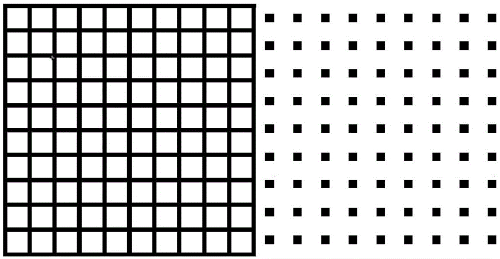
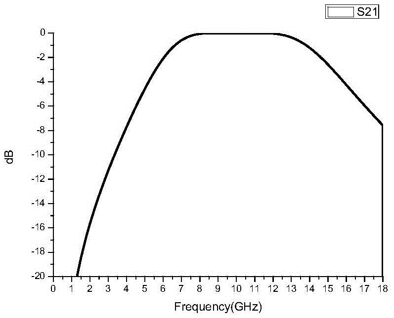
[0033] The designed FSS composite material is a two-layer ceramic material, three-layer resonant structure, the surface resonant structure is a square, and the middle resonant structure is a grid, see figure 1 . Using silicon nitride as the main raw material, it was formed by dry pressing, protected by nitrogen, and kept at 1700°C for 2 hours. The dielectric constant was 3.2 and the density was 1.8g / cm3. 3 The porous silicon nitride ceramic material is a wave-transmitting material substrate, and the ceramic substrate is placed in a high-vacuum unbalanced magnetron sputtering furnace for coating. The sputtering target material Ti has a purity of 99.995%, and the sputtering gas is argon with a purity of 99.999%, the reaction gas is nitrogen, the purity is 99.999%, the DC RF current is 3A, the substrate bias voltage is 150V, the target-base distance is 150mm, the substrate temperature is 260°C, and the sputtering time is 3000S. A titanium nitride high-temperature-resistant reson...
Embodiment 2
[0035] The designed FSS composite material is two-layer ceramic material, three-layer resonant structure, the surface resonant structure is square, and the middle resonant structure is grid. Using silicon nitride as the main raw material, it was formed by dry pressing, protected by nitrogen, and kept at 1700°C for 2 hours. The dielectric constant was 3.2 and the density was 1.8g / cm3. 3 The porous silicon nitride ceramic material is a wave-transparent material matrix, and the difference from Example 1 lies in the change of size. A screen plate is prepared with a 380-mesh screen, and a platinum-resistant material is prepared on the surface of the ceramic matrix by a screen printing process using platinum slurry. High-temperature resonant structure, the substrate printed with resonant structure is heat-treated at 1300°C under a nitrogen protective atmosphere, and the substrate with resonant structure is compounded into a multi-layer wave-transparent composite material through alum...
Embodiment 3
[0037] The designed FSS composite material is a two-layer ceramic material, three-layer resonant structure, the surface resonant structure and the middle resonant structure are the same structure, see Figure 5 . Using silicon nitride as the main raw material, it was formed by dry pressing, protected by nitrogen, and kept at 1700°C for 2 hours. The dielectric constant was 3.2 and the density was 1.8g / cm3. 3 The porous silicon nitride ceramic material is the wave-transparent material matrix. The screen plate is prepared with a 380-mesh screen. Using platinum paste, a platinum high-temperature-resistant resonant structure is prepared on the surface of the ceramic substrate through a screen printing process. The substrate printed with the resonant structure Heat treatment at 1300°C under a nitrogen protective atmosphere, and compound the matrix with a resonant structure into a multi-layer wave-transparent composite material through an aluminum dihydrogen phosphate binder. By tes...
PUM
| Property | Measurement | Unit |
|---|---|---|
| electrical conductivity | aaaaa | aaaaa |
| density | aaaaa | aaaaa |
Abstract
Description
Claims
Application Information
 - R&D
- Intellectual Property
- Life Sciences
- Materials
- Tech Scout
- Unparalleled Data Quality
- Higher Quality Content
- 60% Fewer Hallucinations
Browse by: Latest US Patents, China's latest patents, Technical Efficacy Thesaurus, Application Domain, Technology Topic, Popular Technical Reports.
© 2025 PatSnap. All rights reserved.Legal|Privacy policy|Modern Slavery Act Transparency Statement|Sitemap|About US| Contact US: help@patsnap.com


