High-performance and high-integration-level L-shaped gate-control schottky barrier tunneling transistor

A tunneling transistor, a high-integration technology, applied in semiconductor devices, electrical components, circuits, etc., can solve the problem of weakening the electric field distribution and carrier distribution control ability of the gate to the source region and drain region, and forming Schottky potential Barrier difficulties, difficult to practical Schottky barrier MOSFETs transistors and other issues, to achieve excellent current conduction ability, improve sub-threshold characteristics and conduction ability, good reverse characteristics and static characteristics

Inactive Publication Date: 2015-01-14
SHENYANG POLYTECHNIC UNIV
View PDF5 Cites 3 Cited by
  • Summary
  • Abstract
  • Description
  • Claims
  • Application Information

AI Technical Summary

Problems solved by technology

And it is extremely difficult to form a Schottky barrier on the surface of a heavily doped extrinsic semiconductor, and the heavy doping itself also seriously weakens the gate's ability to control the electric field distribution and carrier distribution of the source and drain regions
Therefore, it is difficult to realize high-performance practical Schottky barrier MOSFETs transistors

Method used


Image

  • High-performance and high-integration-level L-shaped gate-control schottky barrier tunneling transistor
  • High-performance and high-integration-level L-shaped gate-control schottky barrier tunneling transistor
  • High-performance and high-integration-level L-shaped gate-control schottky barrier tunneling transistor

Examples


Embodiment Construction

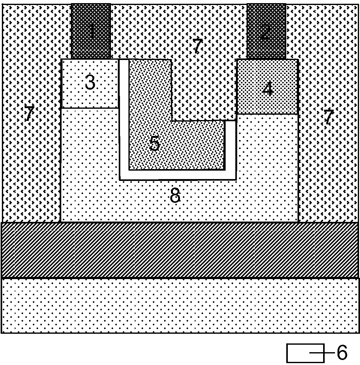
[0033] The invention provides an L-shaped gate-controlled Schottky barrier tunneling transistor with high performance and high integration, without introducing compound semiconductor, silicon germanium or germanium and other materials with narrower band gap than silicon as the tunneling part of the device , but use the Schottky contact barrier formed between the source electrode and the undoped intrinsic silicon source region as the tunneling barrier of the device, and the Schottky barrier height is smaller than the silicon band gap, so The fact that the carrier tunneling probability is higher than the tunneling probability between the conduction band and the valence band of silicon can improve the conductivity of the tunneling transistor, and the gate electrode with the capital letter L is used as the switch control electrode of the device. , on the one hand, the Schottky barrier width of the intrinsic silicon source region is controlled by changing the gate electrode voltage,...


PUM


Abstract

The invention relates to a high-performance and high-integration-level L-shaped gate-control schottky barrier tunneling transistor. A schottky barrier formed between a source electrode and an intrinsic silicon source section is used as a tunneling barrier of a device, the characteristic that the barrier height of the schottky barrier is smaller than the silicon band gap is adopted, on the premise that materials narrower than the silicon band gap do not need to be introduced, the tunneling probability higher than that of a common silicon-material-based PIN type tunneling field effect transistor is achieved, and therefore the subthreshold slope and the electric current conduction capacity of the device are accordingly improved. An L-shaped gate electrode is adopted for controlling an intrinsic silicon channel region with the groove structure characteristics; on one hand, the good control effect on the width of the schottky barrier is achieved; on the other hand, the control effect of the gate electrode on a heavy doping drain electrode region is weakened, and the high-performance and high-integration-level L-shaped gate-control schottky barrier tunneling transistor which has the steep subthreshold slope, the good switching characteristic, the high conduction current, the reversed low leakage current and the quiescent dissipation and is suitable for serving as a deep nanoscale integrated circuit design basic unit is achieved.

Description

technical field [0001] The invention relates to the field of ultra-large-scale integrated circuit manufacturing, and relates to a specific structure, a structural unit and a high-performance high-integration L-shaped gate-controlled Schottky barrier tunneling transistor suitable for ultra-high integration integrated circuit manufacturing. Fabrication method of the array. Background technique [0002] Currently, silicon-based PIN-type tunneling field-effect transistors (TFETs), due to their potential to have better switching characteristics and lower power consumption, may replace MOSFETs as deep nanoscale VLSI logic unit or storage unit. However, compared with MOSFETs, its disadvantage is that the subthreshold slope of the PIN tunneling field effect transistor only partially exceeds that of MOSFETs. As the gate electrode voltage increases, the subthreshold slope decreases, and the forward conduction current flows Small. In addition, the drain region of the PIN type tunne...

Claims


Application Information

Patent Timeline
Patent Type & Authority Applications(China)
IPC IPC(8): H01L29/78H01L29/423H01L29/10
CPCH01L29/0607H01L29/4236H01L29/42376H01L29/7839
Inventor 刘溪靳晓诗揣荣岩
Owner SHENYANG POLYTECHNIC UNIV
Why Eureka
Try Eureka