Manufacturing method for three-dimension controllable silicon based mold
A mold manufacturing, silicon-based technology, applied in the field of surface relief structure layer transfer technology, can solve problems such as high cost and high complexity, achieve stable etching rate, wide range of uses, and reduce production costs
- Summary
- Abstract
- Description
- Claims
- Application Information
AI Technical Summary
Problems solved by technology
Method used
Image

Examples
Embodiment 1
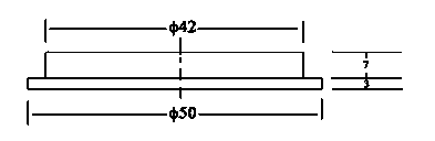
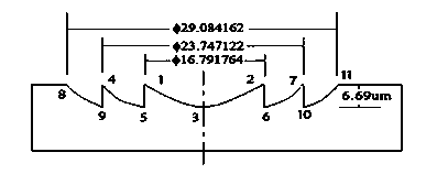
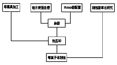
[0037] 1. Design the negative plate of the silicon-based mold according to the actual needs, and use the single-point diamond cutting method to process the designed pattern on the metal copper material, see figure 1 and figure 2 , the depth of the three-dimensional relief structure in this embodiment is 6.69 μm;
[0038] 2. Prepare PMMA solution in anisole according to the ratio of solute to solution mass ratio of 3:10; after the solute is fully dissolved, spin-coat it on the cleaned silicon wafer with a KW-4A / 5 type glue homogenizer, at 90°C Dry for 5 minutes, and form a PMMA film with uniform thickness after drying;
[0039] 3. Transfer the relief structure on the master mold to the silicon-based material coated with PMMA by hot embossing;
[0040] 4. Perform plasma etching on the ICP180 equipment produced by Oxford Instruments Co., Ltd., such as Figure 4 , the position of the intersection point is the optimal gas ratio during etching, and the gas ratio of the intersect...
Embodiment 2
[0042] 1. Design the metal negative plate structure such as Image 6 As shown, the depth of the structure is 6 μm, and the required structure is processed on the metal copper by single-point diamond cutting method, which is used as the negative plate for making the silicon mold;
[0043] 2. Prepare PMMA solution in anisole according to the ratio of solute to solution mass ratio of 5:10; after the solute is fully dissolved, spin-coat it on the cleaned silicon wafer with a KW-4A / 5 type glue homogenizer, at 90°C Dry for 5 minutes, and form a PMMA film with uniform thickness after drying;
[0044] 3. Transfer the relief structure on the negative plate to the silicon-based material coated with PMMA by hot embossing;
[0045] 4. Plasma etching realizes layer transfer, according to the gas ratio SF 6 :O 2 =3.5:10, the two kinds of gases that pass into the reaction chamber are set to be 9sccm and 30sccm respectively, and after 30 minutes of plasma etching, the transfer of the layer...
Embodiment 3
[0047] 1. Design the metal negative plate structure such as Figure 8 As shown, the depth of the structure is 9 μm, and the required structure is processed on the metal copper by single-point diamond cutting method, which is used as the negative plate for making the silicon mold;
[0048] 2. Prepare PMMA solution in anisole according to the ratio of solute to solution mass ratio of 2:10; after the solute is fully dissolved, spin-coat it on the cleaned silicon wafer with a KW-4A / 5 type glue homogenizer, 90°C Dry for 5 minutes, and form a PMMA film with uniform thickness after drying;
[0049] 3. Transfer the relief structure on the negative plate to the silicon-based material coated with PMMA by hot embossing;
[0050] 4. Plasma etching realizes layer transfer, according to the gas ratio SF 6 :O 2 =2.5:10, set the two gases that are passed into the reaction chamber to be 15sccm and 50sccm respectively, after 20 minutes of plasma etching, the layer transfer is completed, and th...
PUM
 Abstract
Description
Claims
Application Information
 - R&D
- Intellectual Property
- Life Sciences
- Materials
- Tech Scout
- Unparalleled Data Quality
- Higher Quality Content
- 60% Fewer Hallucinations
Browse by: Latest US Patents, China's latest patents, Technical Efficacy Thesaurus, Application Domain, Technology Topic, Popular Technical Reports.
© 2025 PatSnap. All rights reserved.Legal|Privacy policy|Modern Slavery Act Transparency Statement|Sitemap|About US| Contact US: help@patsnap.com