A kind of anti-PID solar cell manufacturing method
A technology for solar cells and manufacturing methods, which is applied to circuits, photovoltaic power generation, electrical components, etc., and can solve the problems of reducing the anti-reflection effect of silicon nitride and silicon oxide composite films, reducing the light utilization rate of solar cells, and affecting the efficiency of solar cells, etc. , achieve good surface passivation effect, improve photoelectric conversion efficiency, and excellent anti-PID effect
- Summary
- Abstract
- Description
- Claims
- Application Information
AI Technical Summary
Problems solved by technology
Method used
Image
Examples
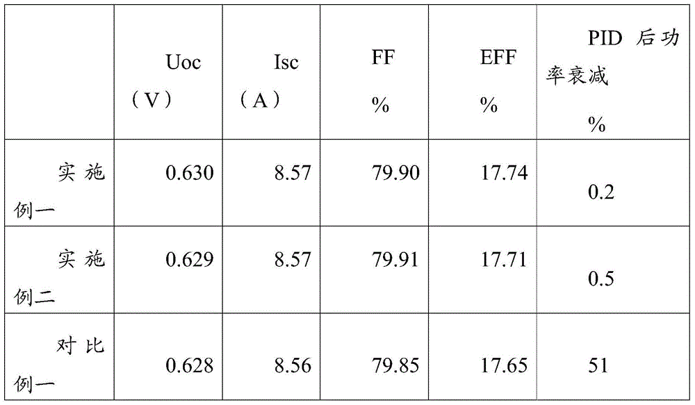
Embodiment 1
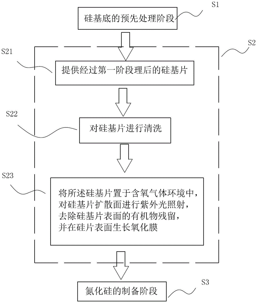
[0055] A kind of method using ultraviolet excitation ozone oxidation to prepare anti-PID thin film, its step comprises:
[0056] (1) Etching and removing the edge of the diffused silicon wafer, cleaning and removing the phosphosilicate glass layer;
[0057] Among them, HF is used for cleaning, the volume concentration of HF solution is 4%, the solution temperature is 20°C, and the cleaning time is 200s;
[0058] (2) After 15 minutes, use ultraviolet rays with a wavelength of 172nm and a light intensity of 100W / m2 to irradiate the diffusion surface of the silicon wafer. The flow rate of 10sccm compressed air is passed around the silicon wafer, and the temperature of the silicon wafer is 20°C. The ultraviolet rays pass through the compressed air to reach the silicon wafer. The distance between the surface of the wafer is 0.5cm, and the processing time is 5s to remove organic residues on the surface of the silicon wafer and grow an oxide film with a thickness of 0.6nm;
[0059] ...
Embodiment 2
[0062] A kind of method utilizing ultraviolet to prepare anti-PID film, its step comprises:
[0063] (1) Etching and removing the edge of the diffused silicon wafer, cleaning and removing the phosphosilicate glass layer;
[0064] Among them, HF is used for cleaning, the volume concentration of HF solution is 5%, the solution temperature is 21°C, and the cleaning time is 55s;
[0065] (2) After 5 seconds, use ultraviolet rays with a wavelength of 185nm and a light intensity of 200W / m2 to irradiate the diffusion surface of the silicon wafer. The flow rate of 8sccm compressed air is passed around the silicon wafer, and the temperature of the silicon wafer is 22°C. The ultraviolet rays pass through the compressed air to reach the silicon wafer. The distance between the surface of the wafer is 0.8cm, and the processing time is 8s to remove organic residues on the surface of the silicon wafer and grow an oxide film with a thickness of 0.8nm.
[0066] (3) After 15 minutes, deposit a...
PUM
| Property | Measurement | Unit |
|---|---|---|
| thickness | aaaaa | aaaaa |
| thickness | aaaaa | aaaaa |
| thickness | aaaaa | aaaaa |
Abstract
Description
Claims
Application Information
 - R&D
- Intellectual Property
- Life Sciences
- Materials
- Tech Scout
- Unparalleled Data Quality
- Higher Quality Content
- 60% Fewer Hallucinations
Browse by: Latest US Patents, China's latest patents, Technical Efficacy Thesaurus, Application Domain, Technology Topic, Popular Technical Reports.
© 2025 PatSnap. All rights reserved.Legal|Privacy policy|Modern Slavery Act Transparency Statement|Sitemap|About US| Contact US: help@patsnap.com


