A kind of integrated circuit flip welding hermetic packaging structure

A technology of integrated circuit and packaging structure, which is applied in the field of integrated circuit reverse welding airtight sealing structure, which can solve the problems of destroying the airtightness of chip packaging and cracking of the covering metal layer, and achieves the protection of airtightness, sealing size and sealing The effect of highly miniaturized and air-tightness guaranteed

Active Publication Date: 2017-01-04
JIANGSU PROVINCE YIXING ELECTRONICS DEVICE GENERAL FACTORY
View PDF12 Cites 0 Cited by
  • Summary
  • Abstract
  • Description
  • Claims
  • Application Information

AI Technical Summary

Problems solved by technology

In the use of high-temperature reflow soldering packaged chips or chips, when the temperature changes alternately, the covering metal layer and the filling resin will generate stress due to the mismatch of thermal expansion coefficients, plus mechanical stress such as clamping, due to the use of evaporation or sputtering methods. The thickness of the covering metal layer is usually only about 10 μm, and the stress can easily cause the covering metal layer to break, thus destroying the package airtightness of the chip

Method used


Image

  • A kind of integrated circuit flip welding hermetic packaging structure
  • A kind of integrated circuit flip welding hermetic packaging structure
  • A kind of integrated circuit flip welding hermetic packaging structure

Examples


Embodiment Construction

[0015] The present invention will be further explained below in conjunction with the accompanying drawings.

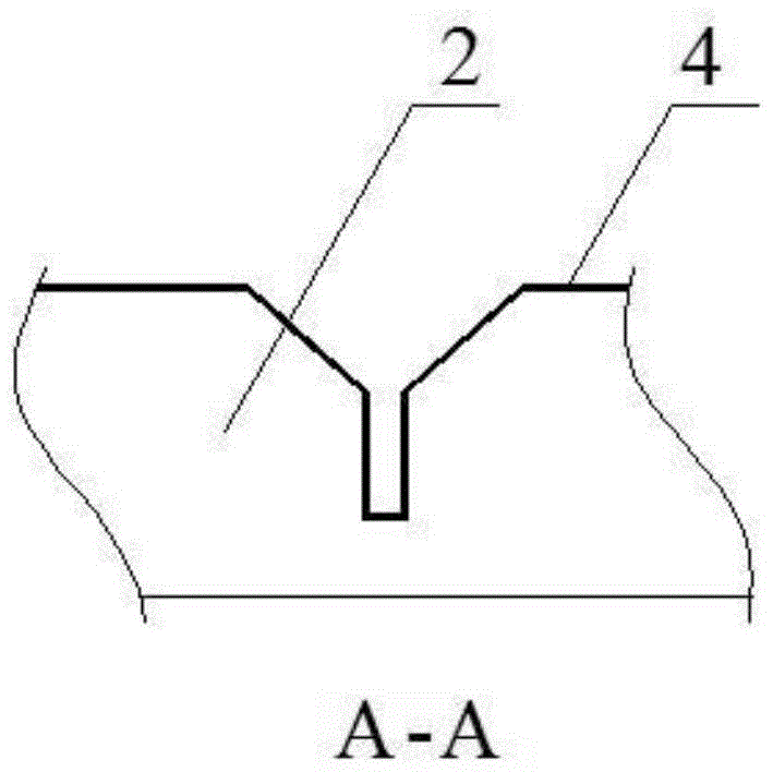
[0016] Such as Figure 5 Shown is a cross-sectional view of the overall integrated circuit upside-down soldering hermetic package structure of the present invention, the structure includes a ceramic substrate 1, a flip-chip 2, a filling resin 3, a metallization layer 4 on the back of the chip, and chip bumps (solder balls) 5. It is composed of annular solder 6 and solder 7, a Kovar sealing cover plate 8, a ceramic metallized sealing ring 9, and an outer terminal pad 10. Wherein, the metallization layer 4 on the backside of the chip generally includes an adhesion layer, a barrier layer, and a soldering layer structure.

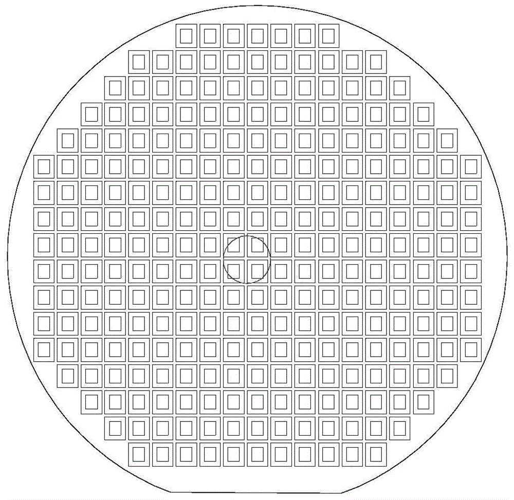
[0017] The chip 2 is formed by thinning the back of the wafer, grooving, chamfering, evaporating or sputtering a multi-layer metallization layer under vacuum, and then cutting with a diamond wheel; the formed metallization layer 4 includes adhesive Ad...


PUM


Abstract

An integrated circuit inverting welding air impermeability packaging structure comprises a ceramic substrate and a flip chip. The flip chip is fixed on the ceramic substrate through chip protruding points, padding resin is arranged between the chip protruding points, and a metallization layer is arranged around the flip chip. The integrated circuit inverting welding air impermeability packaging structure further comprises a kovar sealing cover plate and a ceramic metallization sealing ring. The ceramic metallization sealing ring is arranged on the ceramic substrate on the outer side of the flip chip, and the resin is packaged between the flip chip and the ceramic metallization sealing ring through the kovar sealing cover plate. A covering metal layer in the prior art is replaced by the kovar sealing cover plate which is made of kovar alloy, and the thickness of the kovar sealing cover plate ranges from 100 microns to 200 microns. When the integrated circuit inverting welding air impermeability packaging structure is used in high-temperature reflow welding packaging chips or chips, very small gaps between the kovar sealing cover plate and the padding resin are enough to relieve the size change, caused by temperature change, of the padding resin, and the air impermeability of packaging is protected.

Description

technical field [0001] The invention relates to an integrated circuit flip welding (FC) airtight sealing structure, which belongs to the technical field of microelectronic packaging. Background technique [0002] In order to meet the requirements of thinning, light weight and high performance of integrated circuits, the chip is usually welded to the substrate by flip-down welding process and the bottom is filled, or the chip is bonded to the substrate and then connected by wire bonding, epoxy Resin encapsulation, the integrated circuits packaged by these plastic substrates or ceramic substrates are non-airtight, water vapor and ions in the air diffuse to the surface of the chip through the molecular gap of the resin, and the chip will be damaged under the influence of temperature and humidity over time. Aluminum pressure points and even wiring will corrode and cause electrical performance degradation or even failure. In order to prevent the erosion of water vapor, ions, etc...

Claims


Application Information

Patent Timeline
Patent Type & Authority Patents(China)
IPC IPC(8): H01L23/28H01L23/16
Inventor 马国荣史丽英徐梦娇
Owner JIANGSU PROVINCE YIXING ELECTRONICS DEVICE GENERAL FACTORY
Why Eureka
Try Eureka