A kind of thin-film solar cell and component, and the preparation method of both
A technology of thin-film solar cells and solar cells, applied in electrical components, circuits, photovoltaic power generation, etc., can solve the problems of high manufacturing cost of flexible thin-film batteries, poor substrate temperature resistance, and high equipment requirements, and achieve low cost and low equipment requirements , The effect of low preparation cost
- Summary
- Abstract
- Description
- Claims
- Application Information
AI Technical Summary
Problems solved by technology
Method used
Image
Examples
Embodiment 1)
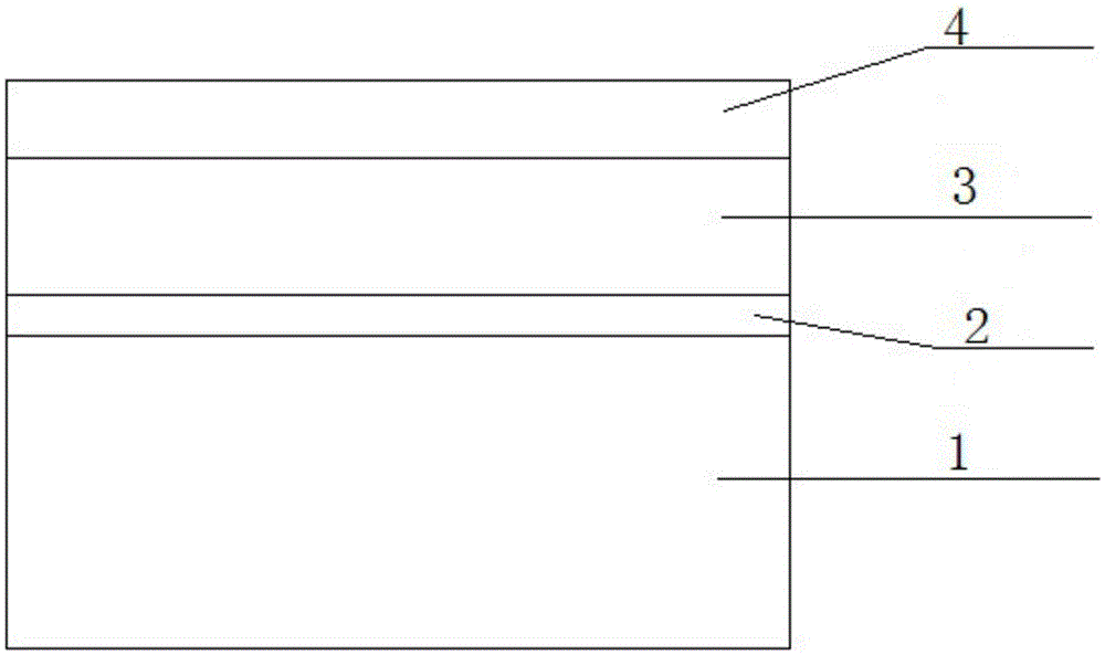
[0044] See figure 1 , the flexible thin film solar cell of the present invention, from bottom to top is flexible transparent substrate 1, thin film solar cell front electrode 2, thin film solar cell body layer 3 and battery back electrode 4; The light transmittance of thin film solar cell front electrode 2 is high At 90%, the surface resistance is lower than 50Ω / sq. The material of the flexible transparent substrate 1 is PI, PET or PEN.
[0045] The preparation steps are:
[0046] Step 1: If Figure 4 As shown, a graphene film is prepared on a temporary substrate 8 as the front electrode 2 of a thin film solar cell; through chemical modification and optimization of the number of layers, the light transmittance of the graphene film is higher than 90%, and the surface resistance is lower than 50Ω / sq; Temporary substrate 8 is copper foil or nickel foil or ruthenium or iridium or silicon or silicon carbide or mica; The method for preparing graphene film is chemical vapor deposi...
Embodiment 2)
[0054] Compared with Example 1, in step one, the graphene surface work function is adjusted by surface modification, improving its contact with the solar cell functional layer; as Figure 6 As shown, the front electrode of the thin film solar cell is in contact with the P layer of the thin film solar cell body layer 3, and the graphene work function is improved to be higher than the work function of the P layer, and the front electrode 2 of the thin film solar cell forms an ohmic contact with the P layer, as shown in Fig. Among them, Wg represents the graphene work function; Wp represents the work function of the battery and the graphene contact functional layer; E refers to the energy level (the probability that the electron is in the state of the energy level); Eo refers to the vacuum energy level of the semiconductor or metal, that is, the electron Ec refers to the conduction band of the semiconductor; Ev refers to the valence band of the semiconductor; between Ec and Ev is ...
Embodiment 3)
[0056] Compared with Example 2, step 2 also includes adding a transition layer 10 between the front electrode 2 of the thin film solar cell and the body layer 3 of the thin film solar cell; if the P layer of the body layer 3 of the thin film solar cell is in contact with the transition layer 10, Then the valence band of the transition layer 10 is equal to the valence band of the P layer of the thin film solar cell body layer 3 in contact with it, and the conduction band is higher than the conduction band of the P layer of the thin film solar cell body layer 3 in contact with it; if What is in contact with the transition layer 10 is the N layer of the thin film solar cell body layer 3, then the conduction band of the transition layer 10 is equal to or lower than the conduction band of the N layer of the thin film solar cell body layer 3 in contact with it, and the valence band is lower than The valence band of the N layer of the thin film solar cell body layer 3 in contact with ...
PUM
 Abstract
Description
Claims
Application Information
 - R&D
- Intellectual Property
- Life Sciences
- Materials
- Tech Scout
- Unparalleled Data Quality
- Higher Quality Content
- 60% Fewer Hallucinations
Browse by: Latest US Patents, China's latest patents, Technical Efficacy Thesaurus, Application Domain, Technology Topic, Popular Technical Reports.
© 2025 PatSnap. All rights reserved.Legal|Privacy policy|Modern Slavery Act Transparency Statement|Sitemap|About US| Contact US: help@patsnap.com


