Radiation-resistant bipolar device and its preparation method

A bipolar device and anti-irradiation technology, applied in the field of anti-irradiation, can solve the problems of poor anti-irradiation ability, achieve high failure threshold, reduce composite leakage current, and improve anti-irradiation ability

Active Publication Date: 2017-03-01
HARBIN INST OF TECH
View PDF3 Cites 0 Cited by
  • Summary
  • Abstract
  • Description
  • Claims
  • Application Information

AI Technical Summary

Problems solved by technology

[0007] The purpose of the present invention is to solve the problem of poor radiation resistance of existing bipolar devices, and propose a radiation-resistant bipolar device and a preparation method of the device based on optimizing the surface structure and concentration of the device base

Method used


Image

  • Radiation-resistant bipolar device and its preparation method
  • Radiation-resistant bipolar device and its preparation method
  • Radiation-resistant bipolar device and its preparation method

Examples


specific Embodiment approach 1

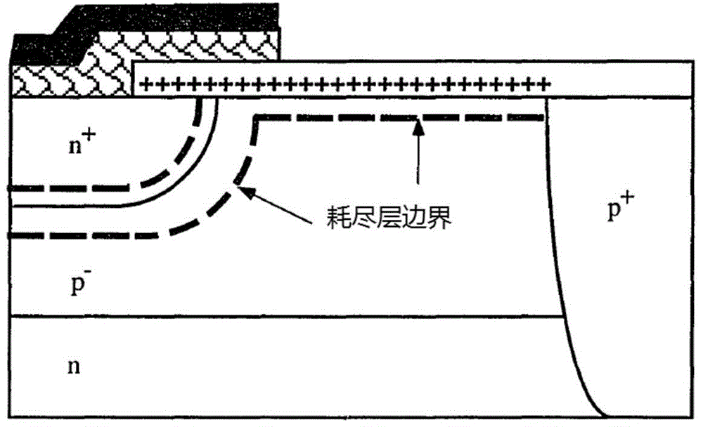
[0026] Specific implementation mode one: combine Figure 4 and Figure 5 Describe this implementation mode. In the radiation-resistant bipolar device described in this implementation mode, a high-doping concentration region centered on the emitter region is provided on the surface of the base region, and the doping concentration of the high-doping concentration region is the body region. 10 to 10,000 times the doping concentration.

[0027] The optimal range of the doping concentration of the high doping concentration region is 10 to 10000 times the doping concentration of the body region.

[0028] The radiation-resistant bipolar device described in this embodiment forms a high doping concentration region around the emitter region on the surface of the base region without affecting the electrical performance parameters of the device. Such as Figure 4 As shown, after radiation damage, the high doping concentration region on the surface of the base region hinders the expansi...

specific Embodiment approach 2

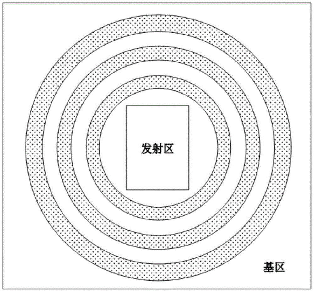
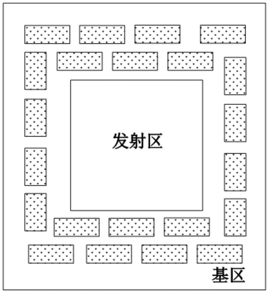
[0030] Specific implementation mode two: combination figure 2 and Figure 5 This implementation mode is described. This implementation mode is a further limitation of the radiation-resistant bipolar device described in the first implementation mode. In this implementation mode, the high doping concentration region is a multi-ring high doping concentration region.

[0031] Depend on Figure 5 It can be seen that, compared with the traditional base structure, the failure threshold of the bipolar transistor with multi-ring high doping concentration regions is 3.7 times higher.

specific Embodiment approach 3

[0032] Specific embodiment three: This embodiment is a further limitation of the radiation-resistant bipolar device described in embodiment two. In this embodiment, the depth of the multi-ring high doping concentration region is 1 of the depth of the emitter region. / 20~1 / 5, the width of the ring is 0.01~10μm, the minimum distance between the boundary of the inner ring and the boundary of the emission area is 0.01~10μm, the distance between two adjacent rings is 0.1~10μm, and the number of rings is 1~10 indivual.


PUM


Abstract

The invention relates to the technology of radiation resisting of bipolar devices, in particular to a radiation resistant bipolar device and a manufacturing method of the radiation resistant bipolar device. The radiation resistant bipolar device and the manufacturing method of the radiation resistant bipolar device aim to solve the problem that an existing the radiation resisting capacity of an existing bipolar device is poor. A high-dosage-concentration region with an emitting region with a center is arranged on the surface of a base region of the bipolar device. The manufacturing method of the radiation resistant bipolar device comprises the steps that after the diffusion or ion injection of the base region is completed and before the diffusion or ion injection of the emitting region is carried out, a radiation resistant strengthening method is carried out; according to the radiation resistant strengthening method, a base region surface doping mask plate is manufactured based on a base region mask plate, foreign ions the same as those in the base region are injected into the surface of the base region based on the mask plate, the injection concentration is 10-10,000 times of the region concentration, and finally annealing treatment is carried out. The surface structure and the doping concentration of the base region are changed, and the failure threshold of the device is improved by 1.4-3.7 times. The device and the manufacturing method are suitable for NPN devices, PNP devices, digital bipolar circuits, simulated bipolar circuits and DA / AD circuits.

Description

technical field [0001] The invention relates to anti-radiation technology of bipolar devices. Background technique [0002] During the flight in orbit, the spacecraft interacts with various charged particles (electrons and protons) in space. These electrons and protons have a strong impact on the performance of electronic devices used in spacecraft, causing ionizing radiation effects, displacement radiation effects, and single event effects. These radiation effects will lead to abnormalities or failures of electronic devices, and even eventually lead to catastrophic accidents in spacecraft. The research results at home and abroad show that different forms of failures will occur on the spacecraft in orbit, which shortens the working life and causes great losses. The results of fault analysis show that the radiation damage effect of space charged particles on electronic devices on spacecraft is an important cause of faults and even accidents. Today, with the development of ...

Claims


Application Information

Patent Timeline
Patent Type & Authority Patents(China)
IPC IPC(8): H01L29/73H01L29/06H01L21/331
CPCH01L29/36H01L29/66234H01L29/73
Inventor 李兴冀杨剑群刘超铭肖景东何世禹
Owner HARBIN INST OF TECH
Why Eureka
Try Eureka