
A Method for Improving Nonlinear Optical Properties Using Nano-Silicon and SiO2 Interface States

A silicon dioxide, interface state technology, applied in nonlinear optics, optics, instruments, etc., can solve the problems of small nonlinear optical coefficient of bulk silicon material, limited adjustment range, technical difficulty, etc., and achieve enhanced nonlinear optical coefficient. , Good controllability and repeatability, cost reduction effect

Inactive Publication Date: 2016-11-16
NANJING UNIV
View PDF4 Cites 0 Cited by
  • Summary
  • Abstract
  • Description
  • Claims
  • Application Information

AI Technical Summary

Problems solved by technology

[0004] Due to the small nonlinear optical coefficient of bulk silicon materials, its application in nonlinear optical devices such as optical switches, optical amplification and optical modulation is limited.
The existing methods of preparing nano-silicon / silicon dioxide films mostly use nano-silicon embedded in the silicon dioxide matrix. Although the nonlinear optical coefficient of the material can be improved, the nonlinear optical coefficient of the material is mainly improved by controlling the size and density of the nano-silicon. Linear optical coefficient, technically more difficult, and the range of adjustment is limited

Method used

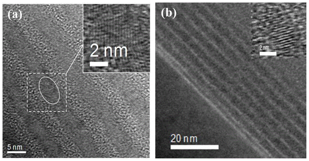
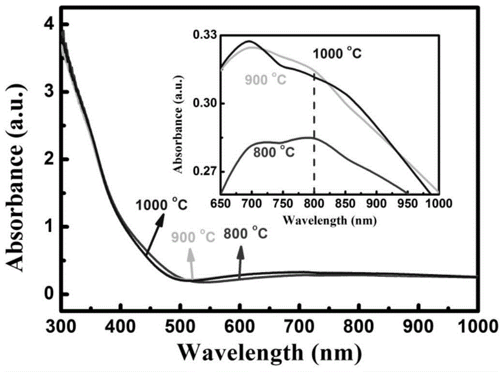
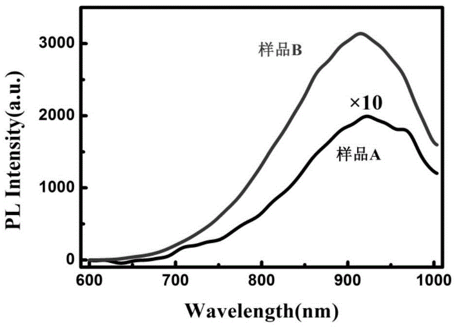

Image

  • A Method for Improving Nonlinear Optical Properties Using Nano-Silicon and SiO2 Interface States
  • A Method for Improving Nonlinear Optical Properties Using Nano-Silicon and SiO2 Interface States
  • A Method for Improving Nonlinear Optical Properties Using Nano-Silicon and SiO2 Interface States

Examples


Embodiment Construction

[0026] The present invention comprises the following steps:

[0027] 1) Using plasma-enhanced chemical vapor deposition technology to prepare amorphous silicon / silicon dioxide multilayer films with controllable sublayers of amorphous silicon, that is, to control the growth of amorphous silicon and in-situ plasma oxidation time to control the amorphous silicon The thickness of the crystalline silicon sublayer; using plasma enhanced chemical vapor deposition technology;

[0028] 1-1. Substrate pretreatment. Before growing the thin film, pretreat the surface of the single crystal silicon substrate or the quartz substrate with argon (Ar), the power of the radio frequency power supply is 50W, and the time is 5 minutes. The purpose of pretreatment is to strengthen the adhesion between the film and the substrate.

[0029] 1-2. Preparation of amorphous silicon / silicon dioxide multilayer film. The amorphous silicon sublayer is deposited by decomposing silane gas, the gas flow rate i...


PUM

PropertyMeasurementUnit
thicknessaaaaaaaaaa
thicknessaaaaaaaaaa

Abstract

The invention provides a method for improving non-linear optical performance by using nanometer silicon and silicon dioxide interface state. The method comprises the following steps of 1) preparing multiple thin film layers alternated by amorphous silicon and silicon dioxide on a monocrystalline silicon substrate or a quartz substrate by using a plasma enhanced chemical vapor deposition technique, controlling the thicknesses of amorphous silicon sub-layers and silicon dioxide sub-layers through controlling the growth time and in-situ plasma oxidation time of the amorphous silicon, controlling the thicknesses of the amorphous silicon sub-layers and the silicon dioxide sub-layers, then forming nanometer silicon quantum dots to acquire materials which have different sizes and densities, wherein 4-16 layers of amorphous silicon and silicon dioxide are prepared ordinarily; 2) performing thermal annealing treatment on the multiple amorphous silicon and silicon dioxide thin film layers. By the method, the non-linear optical coefficient can be enhanced in a larger range, and the non-linear optical performance can be regulated.

Description

Technical field: [0001] The invention relates to the technical field of nonlinear optical devices. Background technique: [0002] Since the 1960s, due to the continuous development of silicon related technologies, especially the introduction of silicon planar technology and microfabrication technology, the production of silicon integrated circuits has been promoted, and because of the corresponding materials, design and manufacturing technologies The advancement of microelectronics technology has made rapid development and opened up a new era of silicon microelectronics technology development. Information technologies such as computer, automatic control and communication developed on this basis have also developed rapidly. However, with the further improvement of integration, the size of the device will be reduced proportionally, and many new effects will appear, such as quantum tunneling effect, short channel effect, RC interconnection delay and other effects, which will a...

Claims


Application Information

Patent Timeline
Patent Type & Authority Patents(China)
IPC IPC(8): G02F1/355
Inventor 徐骏张培张晓伟谭大猛绪欣李伟徐岭余林蔚陈坤基
Owner NANJING UNIV
Learn More