
Method for forming metal gate

A metal gate and dummy gate technology, used in electrical components, semiconductor/solid-state device manufacturing, semiconductor devices, etc., can solve problems such as affecting the stability of transistors and changing the thickness of the interface material layer.

Active Publication Date: 2014-05-14
SEMICON MFG INT (SHANGHAI) CORP
View PDF3 Cites 5 Cited by
  • Summary
  • Abstract
  • Description
  • Claims
  • Application Information

AI Technical Summary

Problems solved by technology

[0007] However, the thickness of the interface material layer (or interface layer) formed in the prior art is easy to change, which affects the stability of the transistor

Method used


Image

  • Method for forming metal gate
  • Method for forming metal gate
  • Method for forming metal gate

Examples


Embodiment Construction

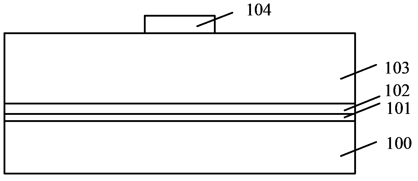
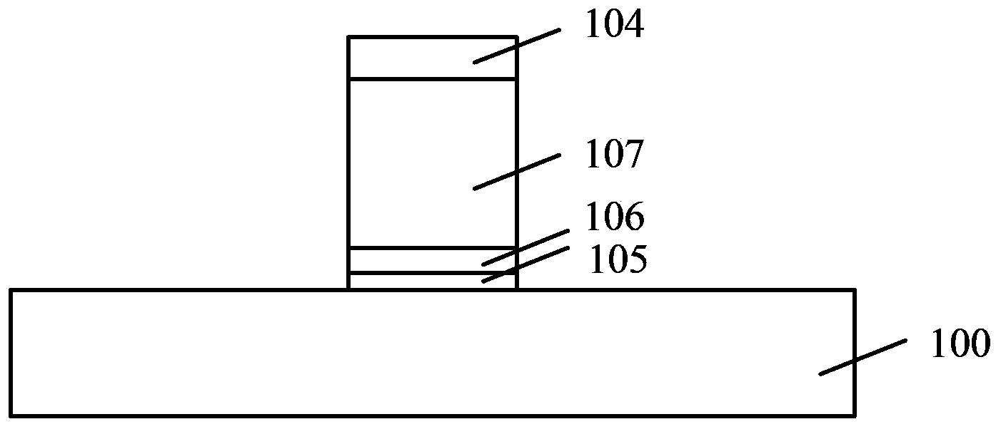
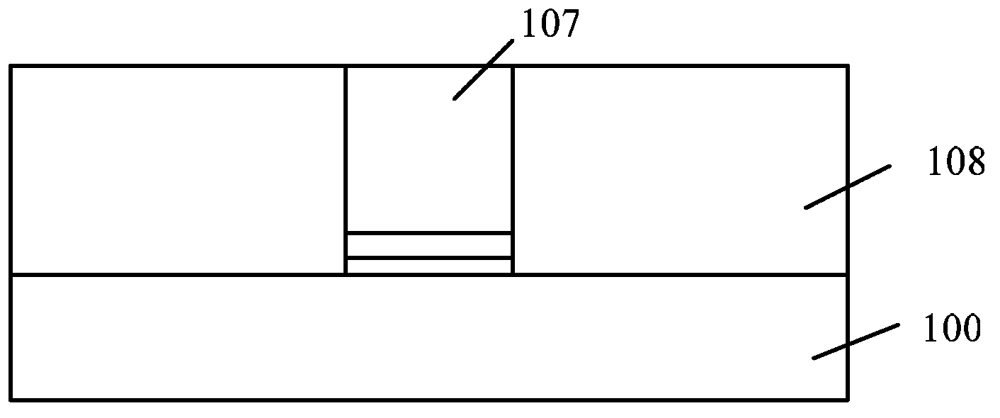
[0029] The inventors found that in the prior art, when making metal gates, the thickness of the interface layer finally formed is always thicker than the thickness of the interface material layer, so that the actual thickness of the interface layer deviates from the designed thickness of the interface layer, which affects the performance of the transistor. performance and stability.

[0030] The inventors have further studied and found that the existing interface material layer is usually formed by a thermal oxidation process. After the interface material layer is formed, the polysilicon layer, hard mask layer, dielectric layer, etc. are all formed by chemical vapor deposition. Chemical vapor deposition During the process, the temperature of the deposition chamber is relatively high (500-800 degrees Celsius). In a high-temperature environment, some oxygen elements will pass through the polysilicon layer and the hard mask layer to reach the surface of the semiconductor substrate...


PUM

PropertyMeasurementUnit
thicknessaaaaaaaaaa

Abstract

A method for forming a metal gate comprises the steps of providing a semiconductor substrate; forming an interface material layer, a high K medium layer and a polycrystalline silicon layer on the surface of the semiconductor substrate; carrying out first nitridation processing on the surface of the polycrystalline silicon layer, and forming a nitrogen silicon compound on the surface of the polycrystalline silicon layer; forming a hard mask layer on the polycrystalline silicon layer after the first nitridation processing, wherein the hard mask layer possesses an opening for exposing the nitrogen silicon compound on the surface of the polycrystalline silicon layer; etching the polycrystalline silicon layer, the high K medium layer and the interface material layer along the opening to form an interface layer, a high K medium layer and a dummy gate; forming an interlayer medium layer on the surface of the semiconductor substrate, wherein the surface of the interlayer medium layer is parallel and level with the top surface of the dummy gate; removing the dummy gate to form a groove, and filling metal in the groove to form the metal gate. The nitrogen silicon compound can prevent an oxygen element from penetrating the polycrystalline silicon layer to react with the silicon on the surface of the semiconductor substrate to form a silicon oxide, and enables the thickness of the interface material layer not to change.

Description

technical field [0001] The invention relates to the field of semiconductor manufacturing, in particular to a method for forming a metal gate. Background technique [0002] With the continuous development of integrated circuit manufacturing technology, the feature size of MOS transistors is getting smaller and smaller. In order to reduce the parasitic capacitance of the gate of MOS transistors and improve the device speed, the gate stack of high K gate dielectric layer and metal gate structure is introduced into MOS transistors. In order to avoid the influence of the metal material of the metal gate on other structures of the transistor, the gate stack structure of the metal gate and the high-K gate dielectric layer is usually fabricated by a “gate last” process. [0003] Figure 1~Figure 4 A schematic cross-sectional structure diagram of a method for forming a metal gate using a "gate-last" process in the prior art. First please refer to figure 1 , providing a semiconduc...

Claims


Application Information

Patent Timeline
Patent Type & Authority Applications(China)
IPC IPC(8): H01L21/28
CPCH01L21/28079H01L29/66545
Inventor 禹国宾
Owner SEMICON MFG INT (SHANGHAI) CORP
Learn More