
Wave length-adjustable light-emitting diode based on gallium-doped zinc oxide nanowire array and manufacturing method thereof

A zinc oxide nanowire, light-emitting diode technology, applied in vacuum evaporation plating, coatings, semiconductor devices, etc., can solve the problems of lattice defects, difficult to increase doping concentration, and decreased device luminescence performance, and reduce the material consumption. Defects, avoidance of material lattice defects, effect of simplifying fabrication methods

Inactive Publication Date: 2014-04-23
HUAZHONG UNIV OF SCI & TECH
View PDF3 Cites 7 Cited by
  • Summary
  • Abstract
  • Description
  • Claims
  • Application Information

AI Technical Summary

Problems solved by technology

[0004] The wavelength tunable light-emitting diodes reported publicly at present all realize the energy band shift of gallium nitride by doping gallium nitride with indium, and the device structure is a planar thin film structure, and a large number of lattice defects are prone to appear during the doping process. , and the doping concentration is difficult to increase, resulting in a decrease in the luminescent performance of the device

Method used

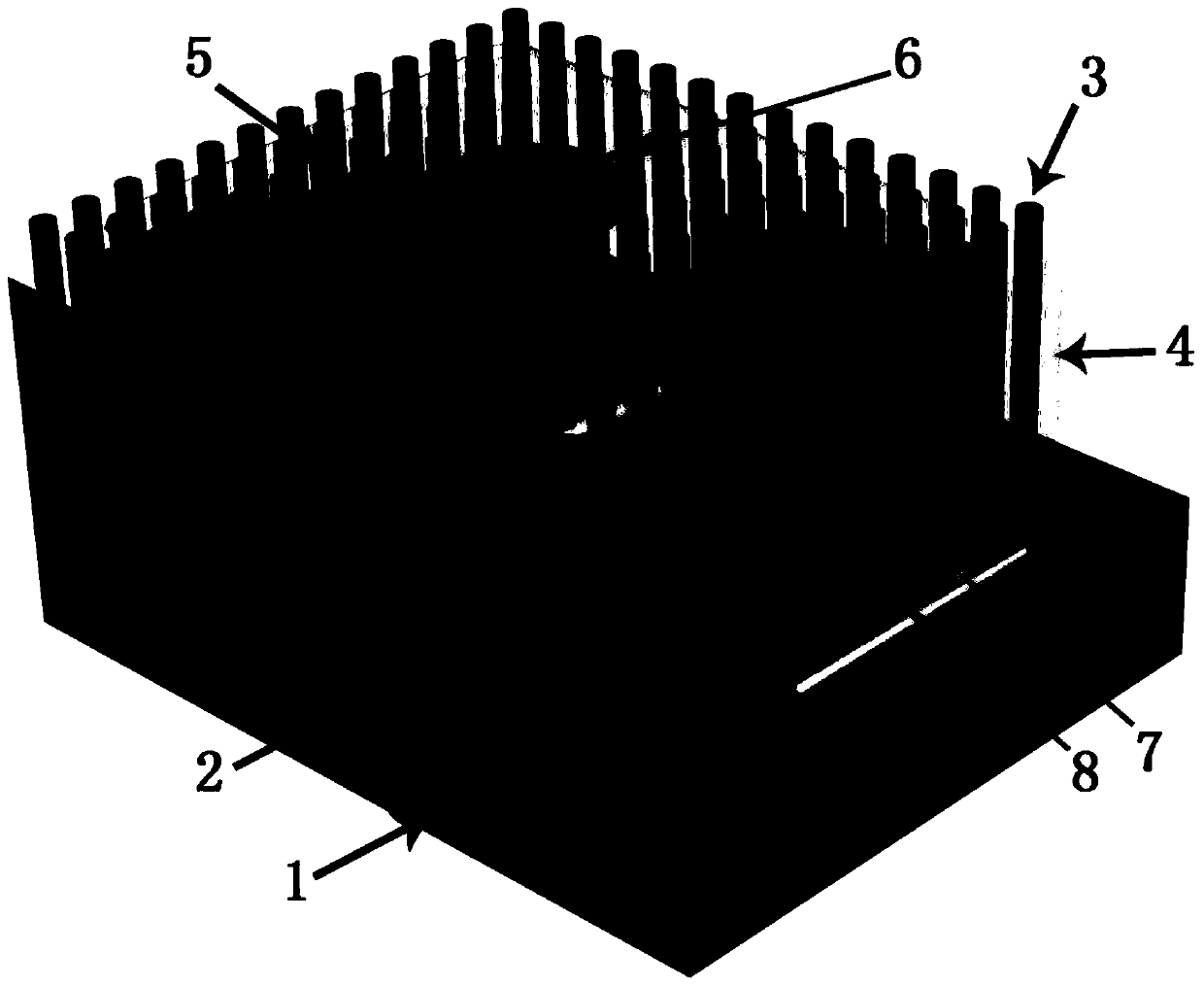
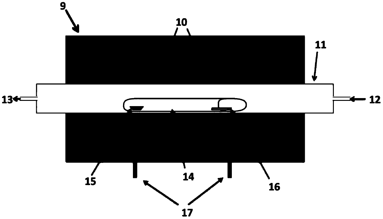
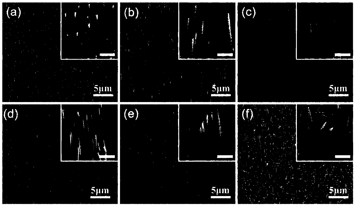

Image

  • Wave length-adjustable light-emitting diode based on gallium-doped zinc oxide nanowire array and manufacturing method thereof
  • Wave length-adjustable light-emitting diode based on gallium-doped zinc oxide nanowire array and manufacturing method thereof
  • Wave length-adjustable light-emitting diode based on gallium-doped zinc oxide nanowire array and manufacturing method thereof

Examples


preparation example Construction

[0049] The preparation method of the wavelength-adjustable light-emitting diode of the gallium-doped zinc oxide nanowire array of the present invention comprises the following steps:

[0050] (1) Provide a p-type conductive substrate;

[0051] (2) On the p-type conductive substrate, the gallium-doped zinc oxide nanowire array is grown by controlling the gallium doping amount of the gallium-doped zinc oxide nanowire array;

[0052] (3) Spin-coat a barrier layer on the grown Ga-doped ZnO nanowire array;

[0053] (4) Etching and removing the barrier layer wrapped on the top of the gallium-doped zinc oxide nanowire array;

[0054] (5) Depositing a top electrode on top of the gallium-doped zinc oxide nanowire array;

[0055] (6) Removing the gallium-doped zinc oxide nanowire array in some areas to expose the p-type conductive substrate, and fabricating the bottom electrode on the exposed p-type conductive substrate.

[0056] Wherein, the step (1) is to prepare a p-type gallium n...


PUM


Abstract

The invention discloses a wavelength-adjustable light-emitting diode based on a gallium-doped zinc oxide nanowire array and a manufacturing method thereof. The wavelength-adjustable light-emitting diode based on the gallium-doped zinc oxide nanowire array comprises a p-type conducting substrate, a gallium-doped zinc oxide nanowire array, a bottom electrode and a top electrode, wherein the gallium-doped zinc oxide nanowire array and the bottom electrode are positioned on the p-type conducting substrate; the top electrode is positioned on the gallium-doped zinc oxide nanowire array. The manufacturing method of the wavelength-adjustable light-emitting diode based on the gallium-doped zinc oxide nanowire array comprises the following steps: providing a p-type conducting substrate; growing a gallium-doped zinc oxide nanowire array on the p-type conducting substrate by controlling the gallium-doping amount of the gallium-doped zinc oxide nanowire array; rotationally coating the grown gallium-doped zinc oxide nanowire array with a blocking layer; etching and removing the blocking layer coated on the top of the gallium-doped zinc oxide nanowire array; depositing the top electrode on the top of the gallium-doped zinc oxide nanowire array; removing a part of the gallium-doped zinc oxide nanowire array to expose the p-type conducting substrate, and manufacturing the bottom electrode on the exposed p-type conducting substrate.

Description

technical field [0001] The invention relates to the field of semiconductor light-emitting devices, in particular to a wavelength-adjustable light-emitting diode based on a gallium-doped zinc oxide nanowire array and a preparation method thereof. Background technique [0002] Semiconductor light-emitting diodes are a new generation of light sources with high energy efficiency, long life and small size. They are widely used in lighting, information communication, display technology and medical technology. The luminous wavelength is an important performance parameter of a semiconductor light-emitting diode, which is determined by the energy band width of the luminescent material. Wavelength-tunable light-emitting diodes have important application prospects in white light lighting and optical display technology, and have become a research hotspot of semiconductor light-emitting diodes. [0003] In the visible light and ultraviolet light regions, gallium nitride materials are al...

Claims


Application Information

Patent Timeline
IPC IPC(8): H01L33/28H01L33/24H01L33/00
CPCH01L33/305C23C14/35H01L33/007
Inventor 高义华张翔晖王玉梅李璐颖苏俊刘逆霜
Owner HUAZHONG UNIV OF SCI & TECH
Learn More