
Leadless ceramic chip carrier packaging structure and process for manufacturing same

A technology of packaging structure and ceramic sheet, which is applied in the manufacture of semiconductor/solid-state devices, electric solid-state devices, semiconductor devices, etc., can solve the problems of easy lack of ceramics in semi-circular holes, low yield, reduced pad pitch, etc., to eliminate Soldering short-circuit problem, easy and thorough cleaning, and the effect of improving the production yield

Inactive Publication Date: 2014-03-26
JIANGSU PROVINCE YIXING ELECTRONICS DEVICE GENERAL FACTORY
View PDF16 Cites 10 Cited by
  • Summary
  • Abstract
  • Description
  • Claims
  • Application Information

AI Technical Summary

Problems solved by technology

When installing, in the traditional technology, when the metallized semicircle hole is connected to the PCB board, due to the large capacitance and inductance and the small gap between the leading ends, the semicircle hole is easy to lack porcelain and short circuit during welding; the metallized semicircle hole is also the overflow of solder. However, as the packaging density increases, the size of the seal shrinks and the pitch of the pads decreases. This structure can no longer meet the needs of the circuit for packaging. The main problems are:
[0003] 1. When brazing metal blocks on ceramics as pads, the yield is very low;
[0004] 2. Using tungsten copper or molybdenum copper as the heat sink, and the structure of the cavity mounted chip cannot guarantee the size of the package structure;
[0005] 3. After the packaged product is assembled, it is difficult to clean around the pad, and it is very difficult to inspect and remove short circuits and excess solder particles

Method used


Image

  • Leadless ceramic chip carrier packaging structure and process for manufacturing same
  • Leadless ceramic chip carrier packaging structure and process for manufacturing same
  • Leadless ceramic chip carrier packaging structure and process for manufacturing same

Examples


Embodiment Construction

[0021] The present invention will be further explained below in conjunction with the accompanying drawings.

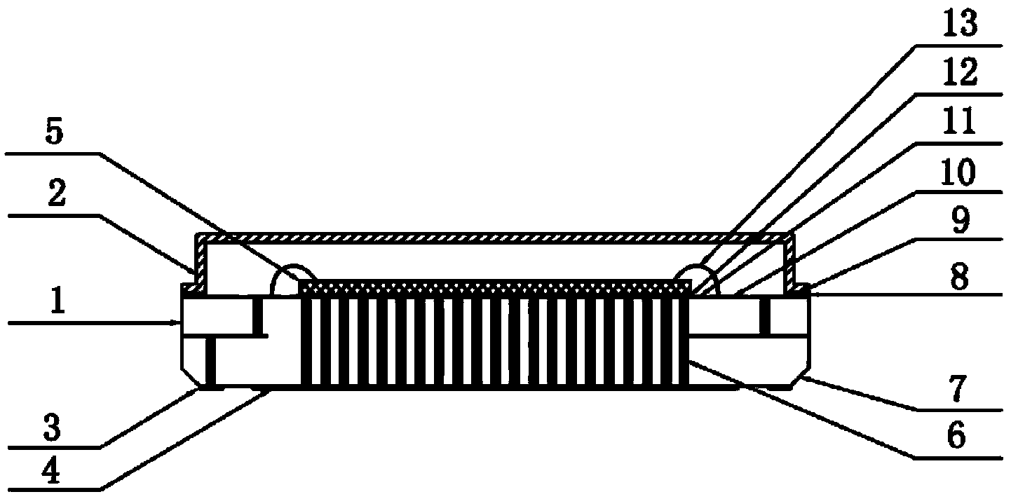
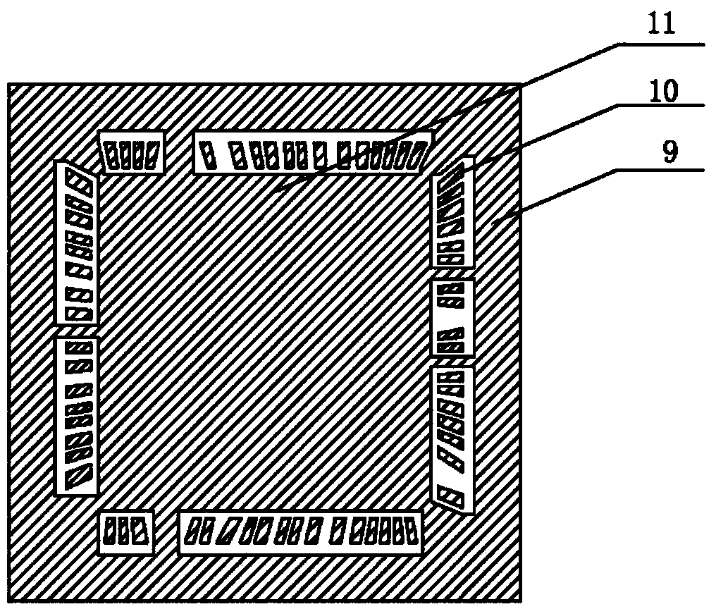
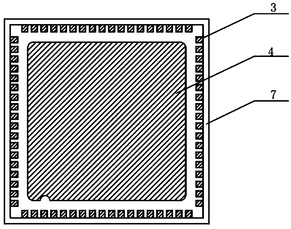
[0022] Such as figure 1 Shown is a schematic structural view of the leadless ceramic chip carrier package of the present invention, which includes a shell 1 and a cover plate 2 , and the cover plate 2 covers the shell 1 . The housing 1 is a multilayer ceramic board, the upper surface of the multilayer ceramic board is provided with a chip bonding area 11 in the center, and a wire bonding area 10 is provided around the chip bonding area 11, and a sealing area 9 is provided around the wire bonding area 10 . Wherein, the sealing area 9 , the wire bonding area 10 , and the chip bonding area 11 are coplanarly arranged. A welding pad 4 is provided at the center of the lower surface of the multilayer ceramic board, and a terminal pad 3 is provided around the pad 4 , and the terminal pad 3 is connected to the wire bonding area 10 . A number of metal via holes 6 are vertical...


PUM


Abstract

The invention discloses a leadless ceramic chip carrier packaging structure and a process for manufacturing the same. The packaging structure comprises a shell and a cover plate. The cover plate covers the shell; the shell is a multilayer ceramic plate, a chip adhesion zone is arranged in the center of the upper surface of the multilayer ceramic plate, and lead bonding zones are arranged on the periphery of the chip adhesion zone; a pad is arranged in the center of the lower surface of the multilayer ceramic plate, and leading-out-end pads are arranged on the periphery of the pad and are connected with the lead bonding zones; a plurality of metal via holes are vertically formed in positions between the upper surface and the lower surface of the multilayer ceramic plate, the upper ends of the metal via holes are connected with the chip adhesion zone, and the lower ends of the metal via holes are connected with the pad; the leading-out-end pads and the pad are of tungsten metallization layer structures. The leadless ceramic chip carrier packaging structure and the process have the advantages that the leading-out-end pads are provided with tungsten metallization layers instead of the traditional pads which are formed by means of brazing metal blocks on ceramics, accordingly, technologies for machining and brazing metal parts and the like can be omitted, the shell manufacturing yield can be increased, and the cost of the shell can be greatly reduced.

Description

technical field [0001] The invention relates to a packaging structure of a leadless ceramic chip carrier and a preparation process thereof, belonging to the technical field of electronic packaging. Background technique [0002] At present, leadless ceramic chip carrier packages in electronic packaging usually use metallized half-through holes as interconnection channels, and the core cavity of the interconnection channels mounts chips; usually brazed tungsten copper or molybdenum copper is used as heat sinks, and flat cover Plate parallel seam welding or alloy solder fusion sealing structure. When installing, in the traditional technology, when the metallized semicircle hole is connected to the PCB board, due to the large capacitance and inductance and the small gap between the leading ends, the semicircle hole is easy to lack porcelain and short circuit during welding; the metallized semicircle hole is also the overflow of solder. However, as the packaging density increase...

Claims


Application Information

Patent Timeline
Patent Type & Authority Applications(China)
IPC IPC(8): H01L23/498H01L23/31H01L21/48
CPCH01L2224/48091H01L2924/15174H01L2924/16152H01L2924/00014
Inventor 马国荣史丽英宋旭峰
Owner JIANGSU PROVINCE YIXING ELECTRONICS DEVICE GENERAL FACTORY
Learn More