Graphene medium-far infrared detector and preparing method thereof

An infrared detector and graphene technology, applied in semiconductor devices, final product manufacturing, sustainable manufacturing/processing, etc., can solve problems such as insufficient absorption rate, affecting graphene transport characteristics and gate electric field adjustable characteristics, etc., to achieve Effects of low gain, low cost, and high infrared light absorption

Inactive Publication Date: 2014-03-12
XIDIAN UNIV
View PDF2 Cites 64 Cited by
  • Summary
  • Abstract
  • Description
  • Claims
  • Application Information

AI Technical Summary

Problems solved by technology

However, graphene can only absorb about 2.3% of the incident light. Although it is already a high absorption rate for a one-way material, it is far from enough for practical light detection.
Of course, if multiple layers of graphene are stacked together, the absorption rate can be effectively improved, but this will inevitably affect the transport characteristics and gate electric field tunable characteristics of graphene.

Method used


Image

  • Graphene medium-far infrared detector and preparing method thereof
  • Graphene medium-far infrared detector and preparing method thereof
  • Graphene medium-far infrared detector and preparing method thereof

Examples


Embodiment

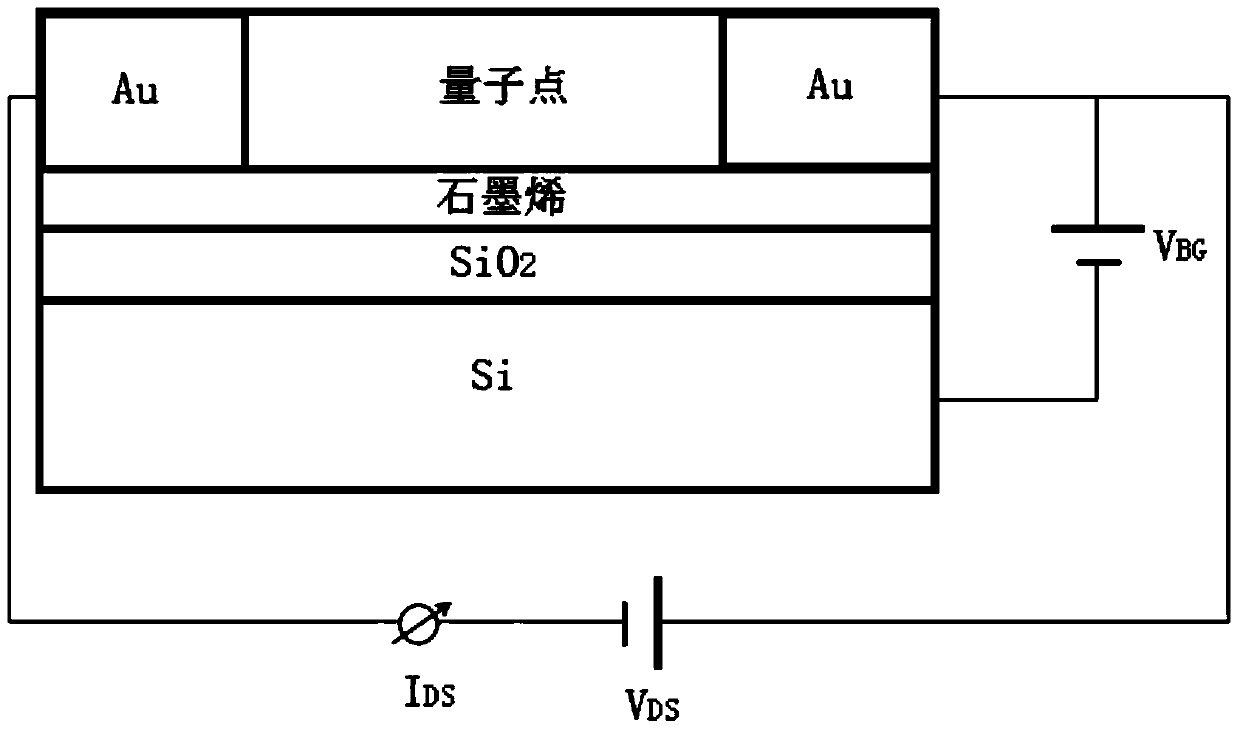
[0024] Embodiment: making InSb quantum dot graphene mid-infrared detector

[0025] When making the InSb quantum dot graphene mid-infrared detector, the present invention takes the following technical solutions:

[0026] 1. Preparation of graphene film: Obtain graphene film through standard mechanical exfoliation process, and the object of exfoliation is highly oriented pyrolytic graphite.

[0027] 2. Transferred graphene film: Transfer the exfoliated graphene to SiO2 / Si substrate with 285nm. Single-layer and double-layer graphene were found by optical microscopy, and Raman scattering spectroscopy was measured by RenishawInviaRaman microscope to determine the actual number of layers of the selected graphene sheet.

[0028] 3. Fabrication of source and drain electrodes: use PMMA as a photoresist, and manufacture drain and source electrodes of the device by electron beam lithography, and the metal of the drain and source electrodes is 5nmTi / 100nmAu.

[0029] 4. Depositing InSb ...


PUM


Abstract

The invention discloses a graphene medium-far infrared detector and a preparing method thereof. The infrared detector comprises a layer of graphene film of which the basic unit is a graphene infrared photoelectric transistor using a colloid quantum dot layer as an optical control top gate. The graphene medium-far infrared probe overcomes the problems of lower absorption rate of graphene to light, and the electricity adjustability of graphene channels is kept, so the graphene medium-far infrared detector can be both optically and electrically bias-controlled. The transistor has ultrahigh infrared absorption rate, inner quantum efficiency, gain and very low noise level and different colloid quantum dot layer materials can be selected according to the difference of detected infrared wavelength ranges. The graphene medium-far infrared detector is easily compatible with the existing silica-based CMOS (complementary metal-oxide-semiconductor transistor) integrated circuit technology, and can realize the large-scale sensor array production with low cost. The successful preparation of the graphene medium-far infrared detector lays a basis for the research on high-performance graphene-based infrared focal plane array sensors.

Description

Technical field: [0001] The invention relates to a structural design and a manufacturing process of an infrared detector, in particular to a structural design and a manufacturing process of a graphene mid-to-far infrared detector. Background technique: [0002] Infrared radiation contains rich objective information, and its detection has attracted much attention. After 70 years of development, infrared detectors have covered short-wave, medium-wave and long-wave ranges, and have been widely used in military and civilian fields. At present, the key technologies of high-performance infrared focal plane array sensors based on pyroelectric, semiconductor quantum wells and quantum dots are mainly mastered by countries such as Europe, America and Japan, forcing domestic research institutions to tackle key problems and catch up with or even surpass existing technologies. [0003] Graphene is a two-dimensional crystal composed of a single layer of carbon atoms. It has excellent mec...

Claims


Application Information

Patent Timeline
IPC IPC(8): H01L31/112H01L31/0352H01L31/18
CPCH01L31/028H01L31/036H01L31/09H01L31/1804Y02P70/50
Inventor 张鹏马中发吴勇庄奕琪赵钰迪冯元博陈祎坤
Owner XIDIAN UNIV
Why Eureka
Try Eureka