
Semiconductor power device

A technology for power devices and semiconductors, applied in the field of semiconductor power devices, can solve the problems of low turn-on speed and turn-off speed, inability to take into account the switching speed, etc., to reduce on-resistance and turn-on power loss, improve performance, and eliminate negative resistance. zone effect

Inactive Publication Date: 2014-02-12
WUXI VERSINE SEMICON CORP
View PDF3 Cites 15 Cited by
  • Summary
  • Abstract
  • Description
  • Claims
  • Application Information

AI Technical Summary

Problems solved by technology

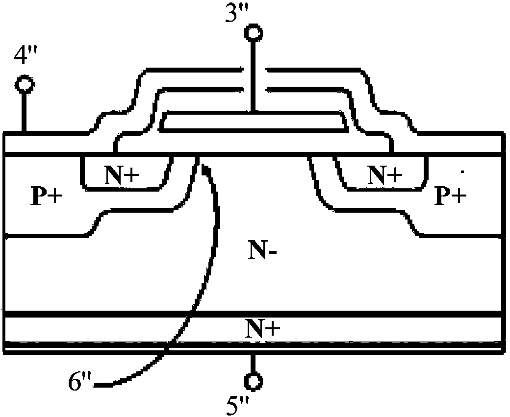
[0005] In view of the above-mentioned shortcomings of the prior art, the purpose of the present invention is to provide a semiconductor power device, which is used to solve the problem that the semiconductor power device in the prior art cannot take into account the very fast switching speed (including turn-on speed and turn-off speed) and The problem of lower on-resistance and turn-on power loss, and at the same time solve the problem that the IGBT in the prior art needs to be connected with an external reverse conduction diode

Method used


Image

  • Semiconductor power device
  • Semiconductor power device
  • Semiconductor power device

Examples


Embodiment 1

[0063] Such as Figure 4 As shown, the present invention provides a semiconductor power device, which at least includes: a drain 101, a drain region 20, a drift region 30, a body region 40, a source region 50, a gate region 60, a heavily doped second conductivity type region 70 , isolation structure 80 , source / emitter 90 , collector 102 , termination structure 110 .

[0064] It should be pointed out that in the first embodiment, the first conductivity type is N-type, and the second conductivity type is P-type, but they are not limited thereto. In other embodiments, the first conductivity type can be P-type , then the second conductivity type is N-type; the material of the drain region 20, the drift region 30, the body region 40, the source region 50, the heavily doped second conductivity type region 70, and the terminal structure 110 is silicon material, but Not limited thereto, in other embodiments, the material of each of the regions may also be silicon carbide or gallium ...

Embodiment 2

[0090] The second embodiment adopts basically the same technical solution as the first embodiment, except that the drift region 30 in the first embodiment is divided into the first drift region 301 and formed in the first drift region 301 in the second embodiment. The second drift region 302 above the region.

[0091] Such as Figure 7 As shown, the present invention provides a semiconductor power device, which at least includes: a drain 101, a drain region 20, a first drift region 301, a second drift region 302, a body region 40, a source region 50, a gate region 60, The second conductivity type region 70 , the isolation structure 80 , the source / emitter 90 , the collector 102 , and the terminal structure 110 are heavily doped. In the following, only the parts different from those in the first embodiment will be described in detail, and the parts that are the same as those in the first embodiment will not be repeated one by one.

[0092] In the second embodiment, the first ...


PUM


Abstract

The invention provides a semiconductor power device. A traditional IGBT and a traditional VDMOS are ingeniously combined to form the novel semiconductor power device provided with a common part and consisting of a basic transverse IGBT and a basic VDMOS. The doping concentration of a re-doped second electric conduction type region is adjusted or a service life controlling method is adopted to decrease first forward breakover current produced by the basic transverse IGBT and meanwhile increase second forward breakover current produced by the basic VDMOS, and the first forward breakover current is smaller than the second forward breakover current. Compared with the traditional IGBT and the traditional VDMOS, the switching speed of the device is improved while the reduction of the breakover resistance loss and the breakover power loss of the device is ensured. By improving a structure of a drifting region, a forward breakover negative resistance region is eliminated, and the performance of the semiconductor power device is improved. The semiconductor power device is applied to the fields of power supplies, solar inverters, motor driving and other fields needing high-voltage and high-frequency switching.

Description

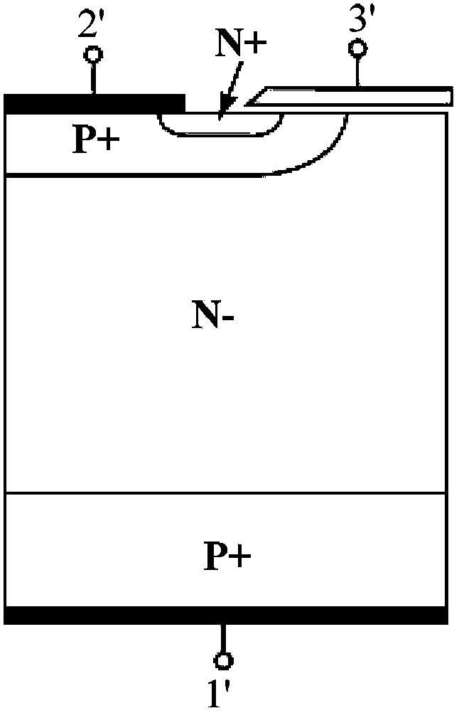
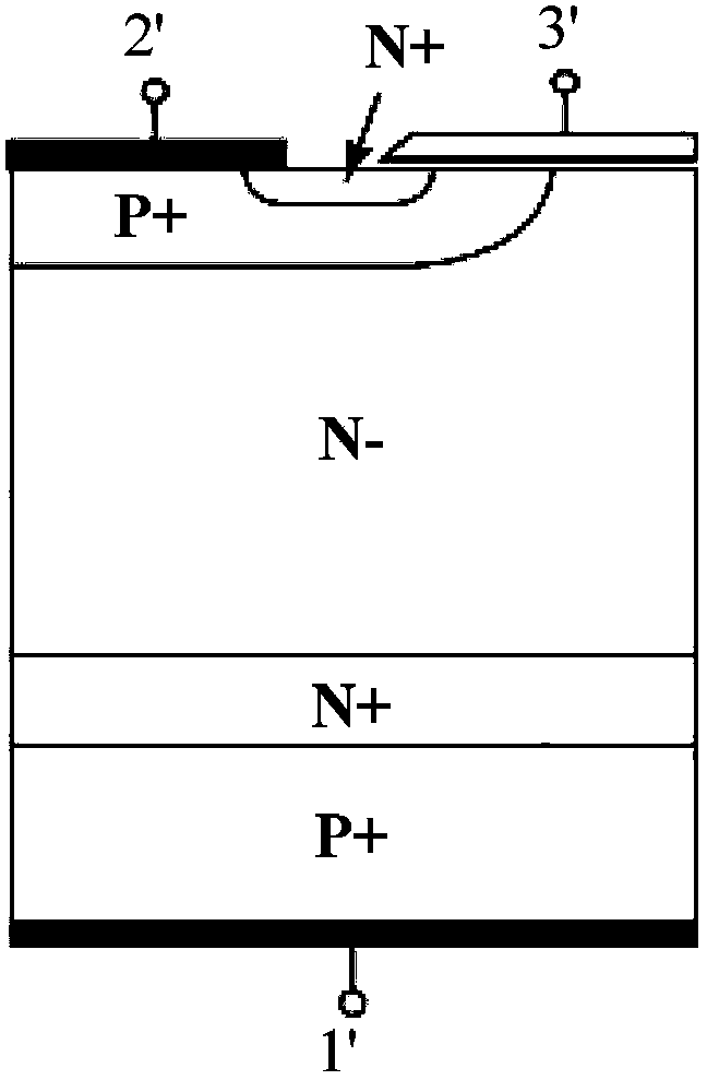
technical field [0001] The invention belongs to the field of semiconductor devices and relates to a semiconductor power device. Background technique [0002] The insulated gate bipolar transistor (Insulated Gate Bipolar Transistor, IGBT) is a composite fully-controlled voltage composed of a bipolar transistor (Bipolar Transistor) and a metal-oxide-semiconductor field-effect transistor (Metal-Oxide-Semiconductor Field Effect Transisitor, MOSFET). Driven power semiconductor devices, and the IGBT is a bipolar device, and two types of carriers (electrons and holes) conduct electricity at the same time. IGBT is generally divided into punch-through (Punch Through, PT), non-punch-through (Non-Punch Through, NPT), electric field stop (electric field stop) type (Field Stop, FS), in which the collector 1', the emitter 2' and gate 3' as figure 1 and figure 2 shown, and figure 1 is a schematic diagram of the structure of NPT-IGBT, figure 2 It is a schematic diagram of the structu...

Claims


Application Information

Patent Timeline
IPC IPC(8): H01L27/06H01L29/739H01L29/78H01L29/06
Inventor 黄勤
Owner WUXI VERSINE SEMICON CORP
Learn More