Method for manufacturing magnesium diboride superconducting thin film micro-structure through annealing
A magnesium diboride and superconducting thin film technology, which is applied in the manufacture/processing of superconductor devices, can solve the problems of inability to form magnesium diboride superconducting thin films with microstructures, poor superconducting properties of thin film microstructures, and precursor films. There are no problems such as microstructure, and the effect of high electrothermal conversion efficiency, short annealing time and high annealing efficiency is achieved
- Summary
- Abstract
- Description
- Claims
- Application Information
AI Technical Summary
Problems solved by technology
Method used
Image
Examples
Embodiment 1
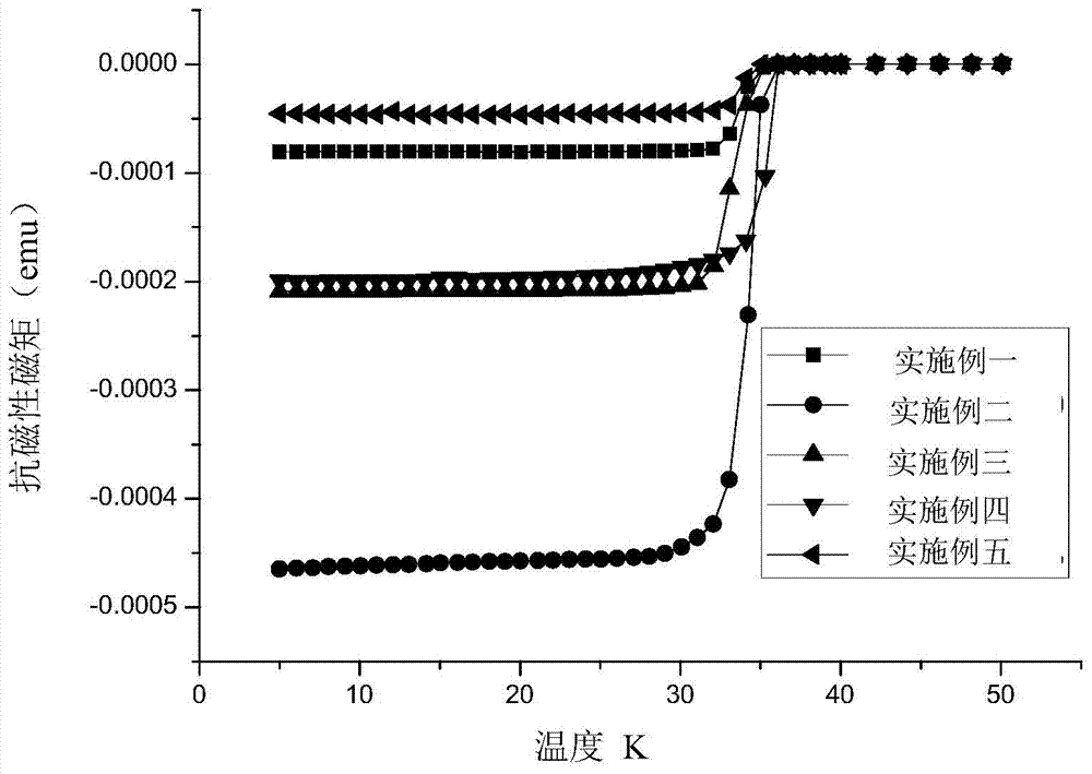
[0038] The preparation of the precursor film in this embodiment is completed in a ZZXS-500 electron beam coating machine, and the electron beam annealing is performed on a self-made EBW-6 electron beam welding machine. The precursor film is [Mg(120 )+B(80 )] 2 , that is, N=2, the film thickness is 40nm, the size of the precursor film is 10.0mm×3.0mm, and the substrate is SiC.
[0039] 1. Precursor film preparation: (1) Fix a SiC bare substrate with a size of 10.0mm×3.0mm on the sample workpiece table; (2) Fix a hollowed-out mask with microstructure on the bare substrate with a spring piece; (3) Place the sample workpiece table in the ZZXS-500 electron beam coating machine, and start vacuuming; (4) Wait for the vacuum degree to be higher than 5×10 -5 After Pa, turn on the quartz crystal thin film coating controller; (5) Evaporate layer B on the substrate until the number on the display panel of the quartz crystal thin film coating controller is 80 (6) Evaporate the Mg la...
Embodiment 2
[0048] The preparation of the precursor film in this embodiment is completed in a ZZXS-500 electron beam coating machine, and the electron beam annealing is performed on a self-made EBW-6 electron beam welding machine. The precursor film is [Mg(120 )+B(80 )] 4 , that is, N=4, the film thickness is 80nm, the size of the precursor film is 10.0mm×3.0mm, and the substrate is SiC.
[0049] 1. Precursor film preparation: (1) Fix a SiC bare substrate with a size of 10.0mm×3.0mm on the sample workpiece table; (2) Fix a hollowed-out mask with microstructure on the bare substrate with a spring piece; (3) Place the sample workpiece table in the ZZXS-500 electron beam coating machine, and start vacuuming; (4) Wait for the vacuum degree to be higher than 5×10 -5 After Pa, turn on the quartz crystal thin film coating controller; (5) Evaporate layer B on the substrate until the number on the display panel of the quartz crystal thin film coating controller is 80 (6) Evaporate the Mg la...
Embodiment 3
[0058] The preparation of the precursor film in this embodiment is completed in a ZZXS-500 electron beam coating machine, and the electron beam annealing is performed on a self-made EBW-6 electron beam welding machine. The precursor film is [Mg(120 )+B(80 )]6 , that is, N=6, the film thickness is 120nm, the size of the precursor film is 10.0mm×3.0mm, and the substrate is Si.
[0059] 1. Precursor film preparation: (1) Fix a Si bare substrate with a size of 10.0mm×3.0mm on the sample workpiece table; (2) Fix a hollowed-out mask with microstructure on the bare substrate with a spring piece; (3) Place the sample workpiece table in the ZZXS-500 electron beam coating machine, and start vacuuming; (4) Wait for the vacuum degree to be higher than 5×10 -5 After Pa, turn on the quartz crystal thin film coating controller; (5) Evaporate layer B on the substrate until the number on the display panel of the quartz crystal thin film coating controller is 80 (6) Evaporate the Mg layer...
PUM
| Property | Measurement | Unit |
|---|---|---|
| Transition temperature | aaaaa | aaaaa |
| Transition temperature | aaaaa | aaaaa |
| Transition temperature | aaaaa | aaaaa |
Abstract
Description
Claims
Application Information
 - R&D
- Intellectual Property
- Life Sciences
- Materials
- Tech Scout
- Unparalleled Data Quality
- Higher Quality Content
- 60% Fewer Hallucinations
Browse by: Latest US Patents, China's latest patents, Technical Efficacy Thesaurus, Application Domain, Technology Topic, Popular Technical Reports.
© 2025 PatSnap. All rights reserved.Legal|Privacy policy|Modern Slavery Act Transparency Statement|Sitemap|About US| Contact US: help@patsnap.com


