Method for manufacturing semiconductor device patterned structure

A manufacturing method and patterning technology, applied in semiconductor/solid-state device manufacturing, photoengraving process of patterned surface, originals for opto-mechanical processing, etc.

Active Publication Date: 2013-11-13
UNITED MICROELECTRONICS CORP
View PDF4 Cites 13 Cited by
  • Summary
  • Abstract
  • Description
  • Claims
  • Application Information

AI Technical Summary

Problems solved by technology

[0005] The purpose of the present invention is to provide a method for fabricating a patterned structure, which can solve the problems in the prior art that the target layer remains or cannot be completely covered.

Method used


Image

  • Method for manufacturing semiconductor device patterned structure
  • Method for manufacturing semiconductor device patterned structure
  • Method for manufacturing semiconductor device patterned structure

Examples


Embodiment Construction

[0039] In order to enable those who are familiar with the technical field of the present invention to further understand the present invention, the preferred embodiments of the present invention are listed below, together with the accompanying drawings, to describe in detail the composition of the present invention and the desired effects .

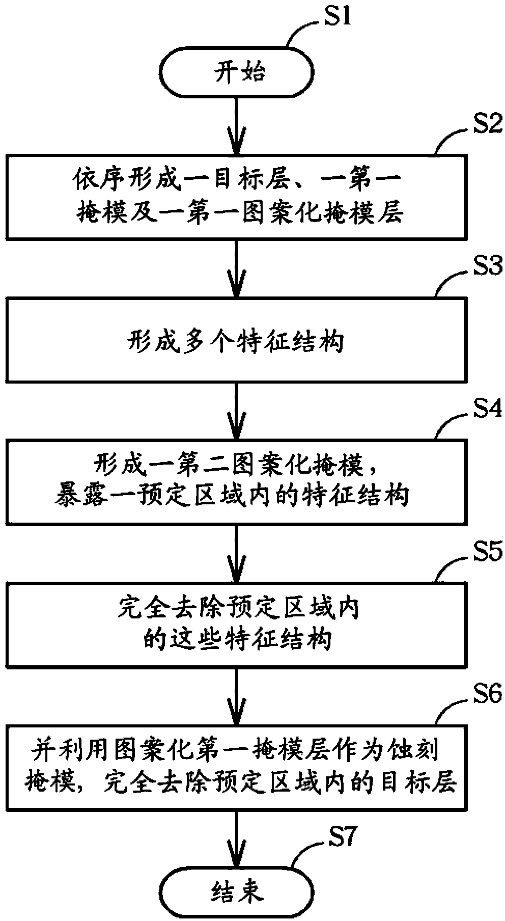
[0040] see figure 1 , figure 1 Shown is a flowchart of a method for fabricating a patterned structure of a semiconductor device according to a preferred embodiment of the double patterning technique (DPT) of the present invention. The process of the present invention is roughly as follows: first, starting with step S1, using step S2 to sequentially form at least a target layer, a first mask layer and a first patterned mask layer on a substrate. Then proceed to step S3 , forming a plurality of feature structures on the substrate by a first etching process, wherein each feature structure includes a patterned first mask and a patterned tar...


PUM

PropertyMeasurementUnit
thicknessaaaaaaaaaa

Abstract

The invention discloses a method for manufacturing a semiconductor device patterned structure. The method includes the steps of firstly, sequentially forming a target layer, a first mask layer and a first patterned mask layer on a substrate, then using the first patterned mask layer as an etching mask, forming a plurality of feature structures on the substrate, wherein each feature structure comprises a first patterned mask layer and a patterned target layer, forming a second patterned mask on the substrate so as to cover a part of the feature structures and expose a preset region, carrying out a second etching manufacturing process, completely eliminating the feather structures in the preset region and the position, in the preset region, of the second patterned mask, finally, carrying out a third etching manufacturing process, using the first pattering mask layers as etching masks, and completely eliminating the positions, which are not covered by the first patterned mask layers, of the target layer.

Description

technical field [0001] The invention relates to the field of a patterned structure, in particular to a method for manufacturing a patterned structure of a semiconductor device. Background technique [0002] The integrated circuit (IC) construction method includes forming patterned features (features) in the substrate or different film layers to form device devices and interconnection structures. In the IC manufacturing process, photolithography (photolithography) manufacturing process is an indispensable technology, which is mainly to form the designed pattern on one or more photomasks, and then through exposure (exposure) and development The (development) step transfers the pattern on the photomask into a photoresist layer on a film layer. Complicated IC structures can be completed with subsequent semiconductor manufacturing process steps such as etching manufacturing process, ion implantation manufacturing process, and deposition manufacturing process. [0003] With the ...

Claims


Application Information

Patent Timeline
Patent Type & Authority Applications(China)
IPC IPC(8): H01L21/311G03F1/80
Inventor 郭龙恩廖俊雄陈炫旭李孟骏
Owner UNITED MICROELECTRONICS CORP
Why Eureka
Try Eureka