Multilayer circuit board structure with embedded components and manufacturing method

A technology of multi-layer circuits and embedded components, which is applied in the manufacture of multi-layer circuits, printed circuits connected with non-printed electrical components, and assembling printed circuits with electrical components. It can improve the tolerance range of the alignment error, simplify the production process, and save the production process steps.

Active Publication Date: 2016-05-18
TRIPOD WUXI ELECTRONICS
View PDF2 Cites 0 Cited by
  • Summary
  • Abstract
  • Description
  • Claims
  • Application Information

AI Technical Summary

Problems solved by technology

Such a manufacturing process is not only complicated in steps, but also, laser drilling from the surface of the circuit board is likely to cause laser offset or alignment errors
In particular, when there are many embedded components or circuit layers in the circuit board, the alignment effect of the conductive vias is less ideal, thus reducing the production yield of the circuit board

Method used


Image

  • Multilayer circuit board structure with embedded components and manufacturing method
  • Multilayer circuit board structure with embedded components and manufacturing method
  • Multilayer circuit board structure with embedded components and manufacturing method

Examples


Embodiment Construction

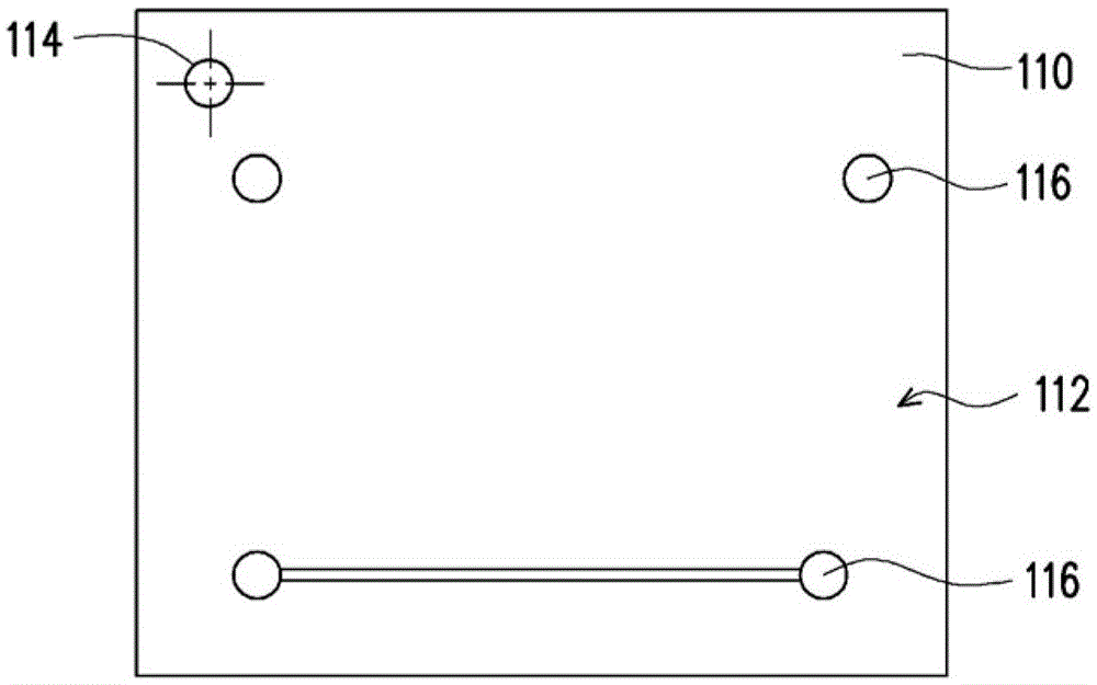
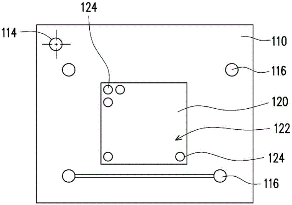
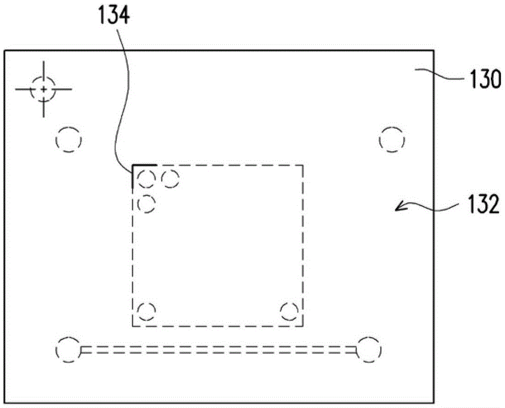
[0050] Figure 1A to Figure 1G It is a schematic top view of the manufacturing process of a multilayer circuit board structure with embedded components according to an embodiment of the present invention. According to the manufacturing method of the multilayer circuit board structure with embedded components in this embodiment, first, please refer to Figure 1A , providing a substrate 110 having a first surface 112 and at least one first alignment mark 114 on the first surface 112 , wherein the first surface 112 of the substrate 110 further has a plurality of first pads 116 . Next, please refer to Figure 1B , disposing at least one semiconductor element 120 (shown as one) on the substrate 110 , wherein the upper surface 122 of the semiconductor element 120 has a plurality of second pads 124 . In this embodiment, the semiconductor element 120 may be an active element, a passive element, a Chip Scale Package (CSP), a circuit board, or any combination thereof. Next, please ref...


PUM


Abstract

The invention discloses a multilayered circuit board structure with a buried element and a manufacturing method. The manufacturing method comprises the following steps of providing a substrate with a first surface and first contraposition marks; arranging semiconductor elements on the substrate; forming a dielectric layer, which covers the semiconductor element, is provided with a second surface and has second contraposition marks, on the substrate; enabling the second contraposition marks to correspond to the semiconductor elements; forming a first through hole group which comprises a plurality of through holes extending to the first surface from the second surface and a second through hole group which comprises a plurality of second through holes extending to the semiconductor elements from the second surface by using the first contraposition marks and the second contraposition marks as contraposition references; forming a wire group on the second surface; and patterning the wire group in two stages so as to respectively obtain a first wire group and a second wire group which are connected with each other.

Description

technical field [0001] The invention relates to a circuit board structure and a manufacturing method, in particular to a multilayer circuit board structure with embedded components and a manufacturing method thereof. Background technique [0002] In the semiconductor industry, the purpose of chip assembly is to protect the bare chip from moisture, heat and noise, and to provide a medium for electrical connection between the bare chip and external circuits. In recent years, with the rapid development of electronic technology and the continuous integration and innovation of high-tech electronic products, traditional semiconductor packaging technology has been unable to meet product function and cost requirements. At present, semiconductor construction technology has moved towards the trend of integrating chips into circuit substrates, so that the entire construction area and volume can be greatly reduced to meet the needs of light, thin, short, high-function, high-speed and hi...

Claims


Application Information

Patent Timeline
Patent Type & Authority Patents(China)
IPC IPC(8): H05K3/46H05K3/30H05K1/18
Inventor 藤川治石汉青范字远杨伟雄
Owner TRIPOD WUXI ELECTRONICS
Why Eureka
Try Eureka