Electrophoretic display and manufacturing method thereof

An electrophoretic display, electrophoretic display technology, applied in the direction of instruments, nonlinear optics, optics, etc., to achieve the effect of avoiding damage, reducing damage, and improving the yield of manufacturing process

Active Publication Date: 2013-06-19
E INK HLDG INC
View PDF3 Cites 0 Cited by
  • Summary
  • Abstract
  • Description
  • Claims
  • Application Information

AI Technical Summary

Problems solved by technology

[0007] The purpose of the present invention is to overcome the defects of the existing electrophoretic display and provide a new electrophoretic display. The technical problem to be solved is to make its electrophoretic display layer cover the active element array and the circuit area of ​​the display area at the same time. The drive circuit, to avoid the drive circuit being damaged by uneven stress, is very suitable for practical

Method used


Image

  • Electrophoretic display and manufacturing method thereof
  • Electrophoretic display and manufacturing method thereof
  • Electrophoretic display and manufacturing method thereof

Examples


Embodiment Construction

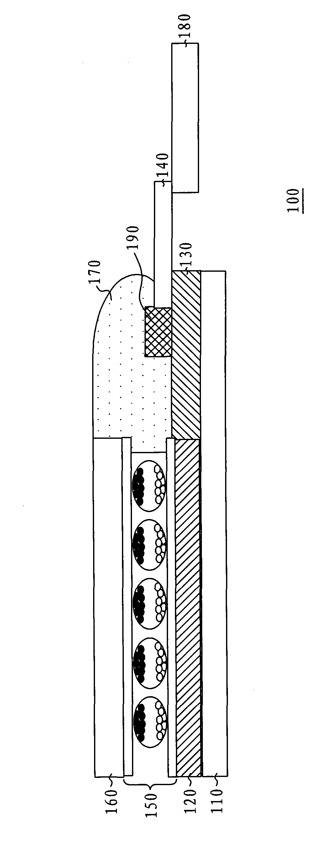
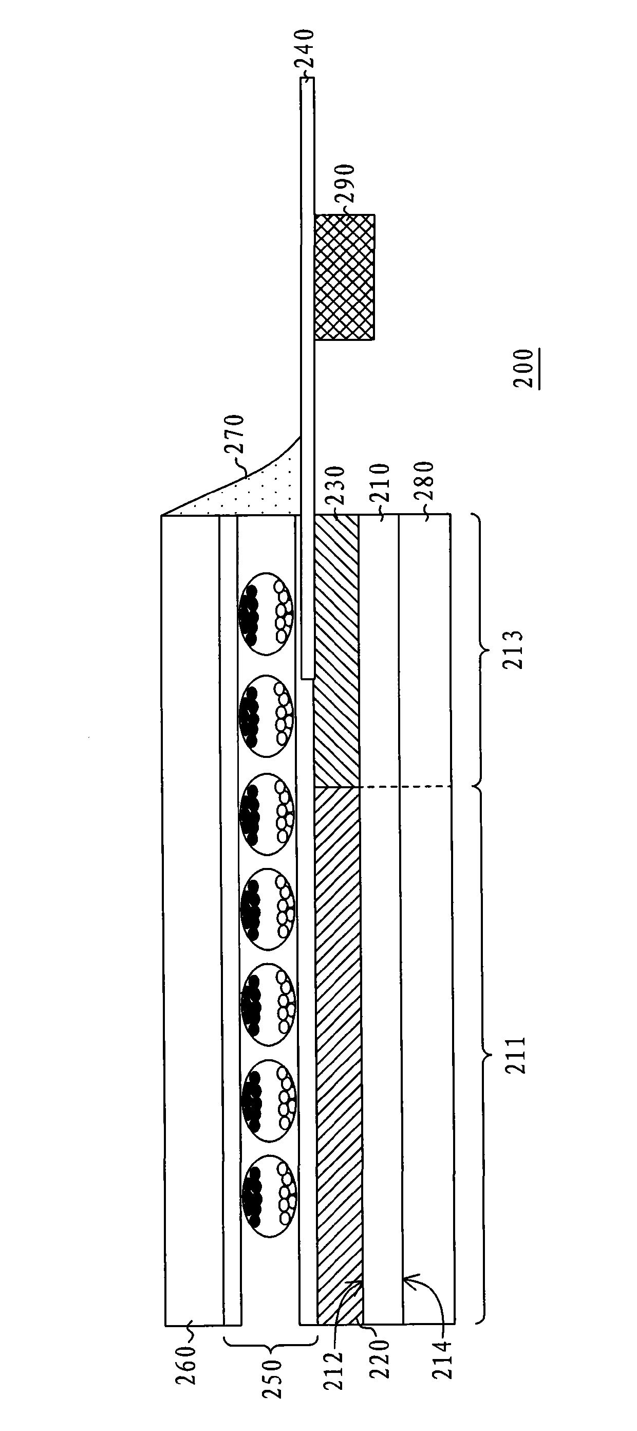
[0053] In order to further explain the technical means and effects of the present invention to achieve the intended purpose of the invention, in conjunction with the accompanying drawings and preferred embodiments, the specific implementation, structure, method, Steps, features and effects thereof are described in detail below.

[0054] figure 2 It is a partial cross-sectional schematic diagram of an electrophoretic display in an embodiment of the present invention. Please refer to figure 2 As shown, the electrophoretic display 200 includes a first substrate 210 , an active element array 220 , a driving circuit 230 , a conductive flexible plate 240 , an electrophoretic display layer 250 , a second substrate 260 and a sealant 270 . Wherein, the first substrate 210 has a first surface 212 , and the first surface 212 has a display area 211 and a circuit area 213 . The first substrate 210 of this embodiment may be a flexible substrate made of plastic materials. Specifically, ...


PUM


Abstract

The invention relates to an electrophoretic display and a manufacturing method thereof. The electrophoretic display comprises a first base plate, an active component array, a driving circuit, a flexible printed circuit, an electrophoretic display layer, a second base plate and a driving chip. The first base plate is provided with a first surface which is provided with a display region and a line region. The active component array is arranged in the display region, the driving circuit is arranged in the line region and is electrically connected to the active component array, and an electric conduction flexible circuit is partially arranged on the first base plate and is electrically connected to the driving circuit. The electrophoretic display layer and the second base plate are arranged on the active component array and the driving circuit sequentially, and the sealing compound is adhered between the second base plate and the electric conduction flexible circuit to tightly seal the electrophoretic display layer between the first base plate and the second base plate. The driving chip is connected with the diving circuit, and the electrophoretic display layer comprises an opening to expose the driving chip. The invention also discloses a manufacturing method of the electrophoretic display.

Description

technical field [0001] The invention relates to a display and a manufacturing method thereof, in particular to an electrophoretic display and a manufacturing method thereof. Background technique [0002] With the advancement of flat panel display technology, more and more electronic products are equipped with displays, especially portable electrical products, such as mobile phones, e-books, digital Camera (digital camera) and personal digital assistant (personal digital assistant, PDA), etc. Since portable electronic products tend to be light in weight and thin in thickness, displays used in portable electronic products also need to have the advantages of light in weight and thin in thickness. [0003] Based on the above, since flexible displays not only have the advantages of light weight and thin thickness, but also have the advantages of being flexible and unbreakable, the manufacture of flexible displays has become an important development trend. At present, the common...

Claims


Application Information

Patent Timeline
Patent Type & Authority Patents(China)
IPC IPC(8): G02F1/167
Inventor 萧博文王子铭庄凯丞蔡渊智吴淇铭黄振勋张永升
Owner E INK HLDG INC
Why Eureka
Try Eureka