Manufacturing method of semiconductor element

一种制作方法、半导体的技术,应用在半导体器件、半导体/固态器件制造、电气元件等方向,能够解决介电层120碎裂、流至其他地方、接触结构122断路等问题

Active Publication Date: 2018-07-10
UNITED MICROELECTRONICS CORP +1
View PDF6 Cites 0 Cited by
  • Summary
  • Abstract
  • Description
  • Claims
  • Application Information

AI Technical Summary

Problems solved by technology

[0007] like figure 1 As shown, when the dielectric layer 120 is formed and cooled, if it is affected by additional stress, the dielectric layer 120 may crack
In this case, the contact structure 122 subsequently formed in the dielectric layer 120 will also cause the conductive layer in the contact structure 122 to flow to other places through these cracks because the dielectric layer 120 has many cracks, which may make the contact Structure 122 creates an open circuit and affects overall DRAM yield

Method used


Image

  • Manufacturing method of semiconductor element
  • Manufacturing method of semiconductor element
  • Manufacturing method of semiconductor element

Examples


Embodiment Construction

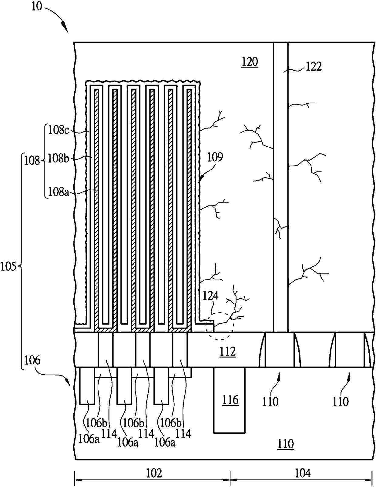
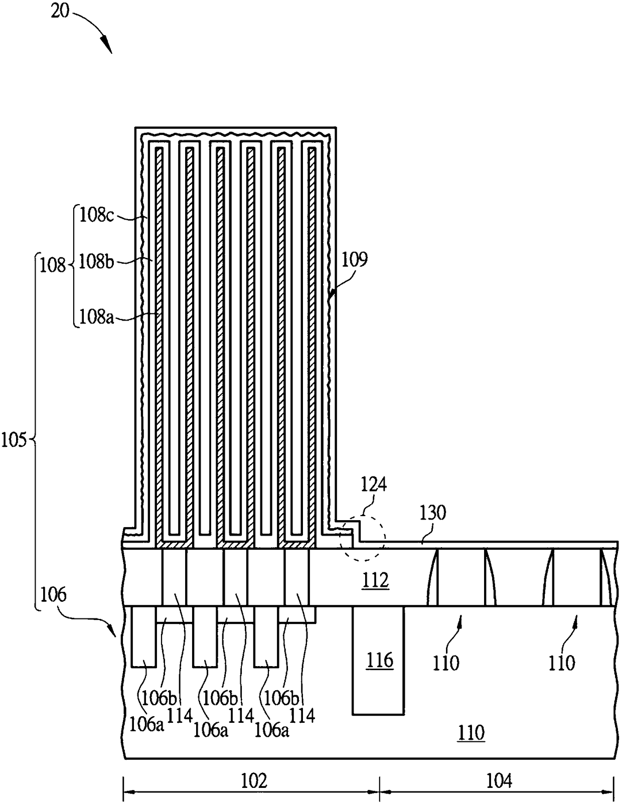
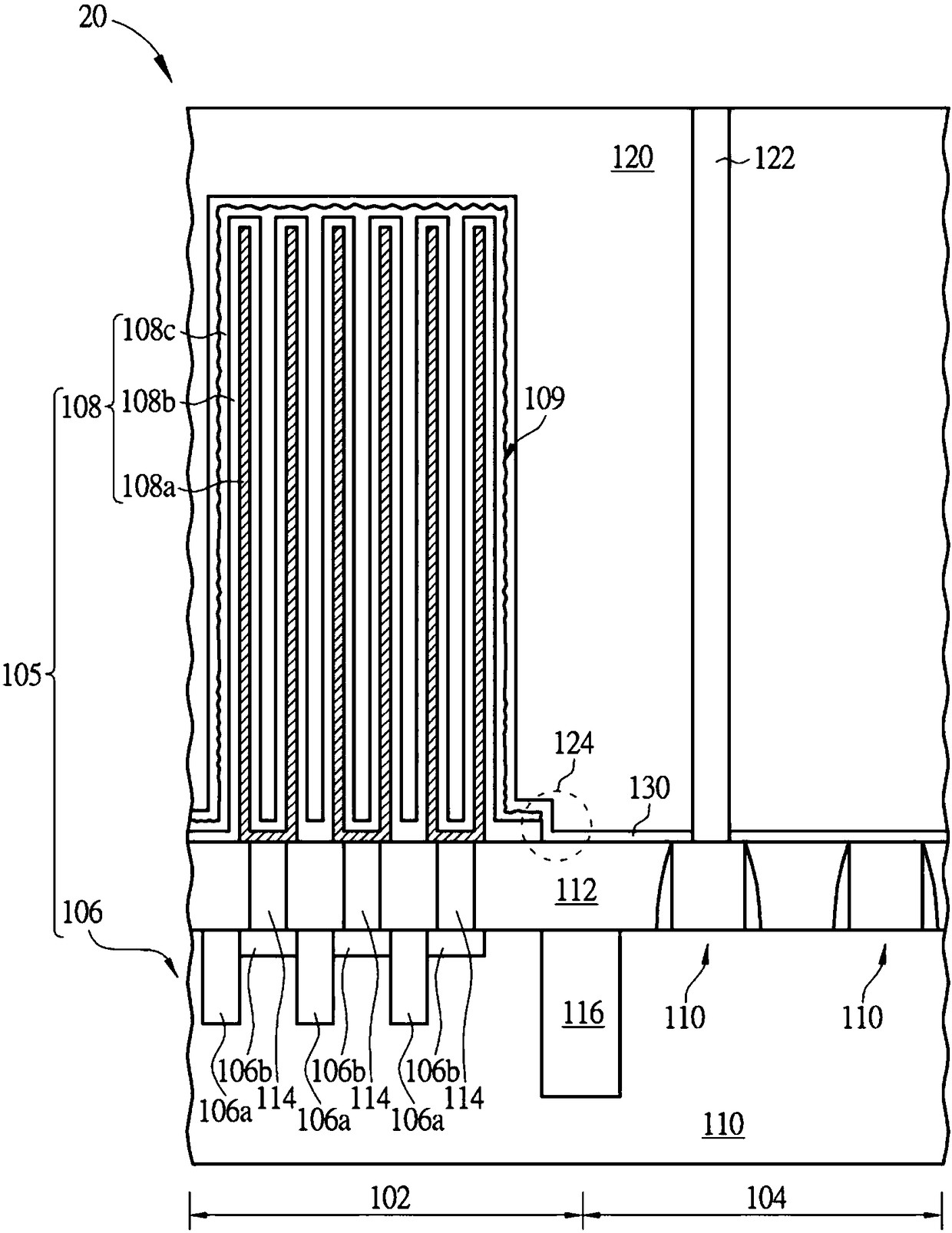
[0041] Please refer to figure 2 as well as image 3 ,in figure 2 as well as image 3 It is a schematic diagram of a dynamic random access memory located at the junction of a storage area and a peripheral area according to the first preferred embodiment of the present invention. First, if figure 2 As shown, a DRAM 20 is provided. Please note that the DRAM 20 here is based on the DRAM 10 mentioned in the background art, and the same components are denoted by the same reference numerals. The substrate 100 includes a storage area 102 and a peripheral area 104 respectively, and the storage area 102 includes at least a plurality of first transistors 106 and capacitors 108 , and the peripheral area 104 includes at least a plurality of second transistors 110 . Components that are not specifically mentioned here and in the following are the same as the DRAM 10 mentioned in the background art, and will not be further described here.

[0042] Please refer to figure 2, after the...


PUM


Abstract

The invention discloses a manufacturing method of a semiconductor element, which at least comprises the steps of firstly providing a substrate, wherein the substrate is internally defined with a storage region and a peripheral region, the storage region contains a plurality of storage units, each storage unit at least comprises a first transistor and a capacitor structure, the peripheral region contains at least one second transistor; then forming a first insulating layer in a mode of atomic layer deposition in the storage region and the peripheral region, wherein the first insulating layer atleast covers the capacitor structure of each storage unit in the storage region and the second transistor in the peripheral region; then forming a second insulating layer which covers the first insulating layer; and forming a contact structure in the second insulating layer in the peripheral region, wherein the contact structure is at least electrically connected with the second transistor.

Description

technical field [0001] The invention relates to the field of semiconductor manufacturing technology, in particular to a method for improving the problem of dielectric layer fragmentation in dynamic random access memory. Background technique [0002] Dynamic random access memory (DRAM for short hereinafter) is a main volatile memory, and is an indispensable key component in many electronic products. DRAM is composed of a large number of memory cells to form an array area for storing data, and each memory cell is composed of a metal oxide semiconductor (MOS) transistor connected in series with a capacitor. [0003] Wherein, the capacitor is located in the storage area, and there is a peripheral area beside the storage area, and the peripheral area includes other transistor elements and contact structures. Generally speaking, the capacitor located in the storage area has a larger height, so it has better charge storage efficiency, but at the junction of the storage area and th...

Claims


Application Information

Patent Timeline
Patent Type & Authority Applications(China)
IPC IPC(8): H01L27/108
CPCH10B12/01H10B12/30H10B12/09H01L28/87H01L28/91H01L21/0228H01L21/02348H10B12/318H10B12/033H01L21/0217H01L21/76825H01L21/02164H01L21/76834H01L21/02112H01L21/823475H10B12/34H10B12/50
Inventor 陈美玲刘玮鑫陈意维张家隆李瑞珉张景翔吴姿锦邹世芳
Owner UNITED MICROELECTRONICS CORP
Why Eureka
Try Eureka