
Epoxy resin composition for semiconductor encapsulation and semiconductor device

A technology of epoxy resin and semiconductor, which is applied in the direction of semiconductor devices, semiconductor/solid-state device components, electric solid-state devices, etc. It can solve the problems of low reliability of moisture resistance, increased resistance of joints, disconnection of joints, etc., and achieve reliability High, moisture-resistant reliability improvement effect

Inactive Publication Date: 2013-07-24
SUMITOMO BAKELITE CO LTD
View PDF8 Cites 2 Cited by
  • Summary
  • Abstract
  • Description
  • Claims
  • Application Information

AI Technical Summary

Problems solved by technology

[0006] However, when the semiconductor element to which the above-mentioned copper wire is connected is sealed with a general epoxy resin composition, the humidity resistance reliability (HAST: Highly Accelerated Temperature & Humidity Test) of the semiconductor device may decrease.
[0007] According to the knowledge of the present inventors, in a semiconductor device with low moisture resistance reliability, due to corrosion of the junction between the electrode pad on the semiconductor element and the copper wire, the resistance of the junction increases or the junction is disconnected.

Method used


Image

  • Epoxy resin composition for semiconductor encapsulation and semiconductor device
  • Epoxy resin composition for semiconductor encapsulation and semiconductor device
  • Epoxy resin composition for semiconductor encapsulation and semiconductor device

Examples


Embodiment 1)

[0147] Epoxy resin B (6.55 parts by mass), curing agent A (6.20 parts by mass), fused spherical silica (86.00 parts by mass) as a filling material, curing accelerator (0.20 parts by mass), coupling agent (0.25 parts by mass parts), carbon black (0.30 parts by mass) as a colorant, and carnauba wax (0.50 parts by mass) as a mold release agent, mixed using a mixer at 15 to 28°C, followed by roller kneading at 70°C to 100°C . After cooling, it was pulverized to obtain an epoxy resin composition.

Embodiment 2~4、 comparative example 1、2

[0149] According to the compounding of the epoxy resin composition for semiconductor sealing described in Table 1, it carried out similarly to Example 1, and obtained the epoxy resin composition for semiconductor sealing. All the blends shown in Table 1 are parts by mass.

[0150] Manufacturing of semiconductor devices:

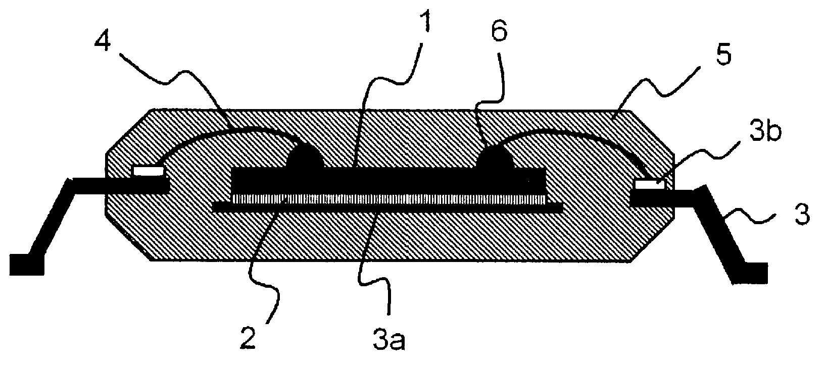
[0151] A TEG (TEST ELEMENT GROUP: Test Element Group) chip (3.5mm×3.5mm) with aluminum electrode pads and a 352-pin BGA (a substrate with a thickness of 0.56mm, bismaleimide triazine resin / glass cloth substrate) , the package size is 30mm×30mm, the thickness is 1.17mm), the chip pad part is bonded, and the aluminum electrode pad of the TEG chip and the electrode pad of the substrate are connected in a daisy chain using copper wire 4N (copper purity 99.99% by mass) for wire bonding with a wire pitch of 80 μm. Using a low-pressure transfer molding machine ("Y series" produced by TOWA), it is made from any of Examples 1 to 4 and Comparative Examples 1 to 2 und...


PUM

PropertyMeasurementUnit
diameteraaaaaaaaaa
softening pointaaaaaaaaaa
particle diameteraaaaaaaaaa

Abstract

Disclosed is a highly reliable semiconductor device with more reliable moisture resistance. The disclosed epoxy resin composition for semiconductor encapsulation is used in the manufacture of semiconductor devices encapsulating both a semiconductor element mounted on a circuit substrate or a leadframe having a die pad unit, and a metal wire electrically connecting an electrical junction provided on the aforementioned circuit substrate or leadframe and an electrode pad provided on the aforementioned semiconductor element. The aforementioned epoxy resin composition for semiconductor encapsulation contains (A) an epoxy resin, (B) a curing agent and (C) an inorganic filler, wherein the aforementioned epoxy resin (A) has a main peak area greater than or equal to 90% of the total area of all peaks, measured by the gel permeation chromatography area method.

Description

technical field [0001] The present invention relates to an epoxy resin composition for semiconductor sealing and a semiconductor device sealed therewith. [0002] this application claims priority based on Japanese Patent Application No. 2010-260913 for which it applied in Japan on November 24, 2010, and uses the content here. Background technique [0003] Conventionally, electronic components such as diodes, transistors, and integrated circuits have been mainly sealed with cured epoxy resin compositions. Especially in integrated circuits, epoxy resin compositions are used that contain epoxy resins, phenolic resin curing agents, and inorganic fillers such as fused silica and crystalline silica, and are excellent in heat resistance and moisture resistance. However, in recent years, in the market trend of miniaturization, light weight, and high performance of electronic equipment, the high integration of semiconductor elements has been progressing year by year, and the surface...

Claims


Application Information

Patent Timeline
Patent Type & Authority Applications(China)
IPC IPC(8): C08L63/00C08G59/24C08K3/00H01L23/29H01L23/31
CPCH01L2224/45124H01L23/3114A61K8/8152H01L24/45H01L2224/05624H01L2224/32245A61Q1/04H01L23/295H01L2224/48247A61K8/92C08G59/20H01L2224/45144H01L2224/73265H01L23/293H01L2224/45147H01L2924/01015C08K5/103H01L2224/48624H01L2224/45015H01L2224/48824H01L2224/48724H01L24/73H01L2924/14A61K8/375A61K8/8111A61K8/8158A61K8/06A61K2800/48H01L2924/181H01L2924/00012H01L2924/00014H01L2924/00015H01L2924/00C08L63/00C08K3/00C08G59/24H01L23/29H01L23/31
Inventor 伊藤慎吾
Owner SUMITOMO BAKELITE CO LTD
Learn More