Surface treatment technology for ceramic substrate of LED (light-emitting diode) area light source
A technology of LED surface light source and ceramic substrate, which is applied in the direction of electrical components, circuits, semiconductor devices, etc., can solve the problems of reducing the ability to maintain light efficiency, achieve the effects of improving long-term stability, increasing reflectivity, and reducing light attenuation
- Summary
- Abstract
- Description
- Claims
- Application Information
AI Technical Summary
Problems solved by technology
Method used
Image
Examples
Embodiment 1
[0021] (1) Clean the alumina ceramic substrate with fixed LED chips and bonding wires on the surface with deionized water, and then dry it in an oven at 120°C for 30 minutes;
[0022] (2) Carry out radio frequency treatment to the alumina ceramic substrate obtained in step (1) in a plasma cleaning machine, the radio frequency power is 250W, the Ar gas flow rate is 20 SCCM, and the treatment time is 1min;
[0023] (3) KER-2500 (silica gel, produced by Shin-Etsu Chemical), TiO 2 , SiO 2 Mix it with YAG-04 (yellow fluorescent powder, produced in the United States) at a weight ratio of 1:5:0.08:0.15, and stir in a vacuum defoaming mixer for 10 minutes;
[0024] (4) Cover the mask plate on the alumina ceramic substrate treated in step (2), use the mask plate to cover and fix the LED chip and bonding wire area, and apply the mixture obtained in step (3) by screen printing On a ceramic substrate with a mask;
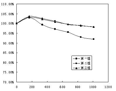
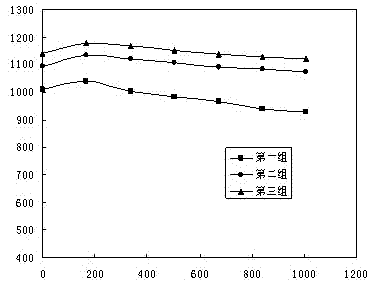
[0025] (5) Remove the mask to get the following figure 1 As shown in t...
Embodiment 2
[0028] (1) Clean the alumina / aluminum nitride composite ceramic substrate with fixed LED chips and bonding wires on the surface with deionized water, and then dry it in an oven at 80°C for 60 minutes;
[0029] (2) Perform radio frequency treatment on the aluminum oxide / aluminum nitride composite ceramic substrate obtained in step (1) in a plasma cleaning machine, the radio frequency power is 150W, the Ar gas flow rate is 35 SCCM, and the treatment time is 3min;
[0030] (3) OE-6650 (silica gel, produced by Dow Corning, USA), ZrO 2 , SiO 2 , Y4156 (green silicate phosphor, produced by Intel America) and BR-102D (nitride red phosphor, produced by Mitsubishi Chemical, Japan) are mixed together in a weight ratio of 1:2:0.01:0.015:0.005. Stir in a vacuum defoaming mixer for 5 minutes;
[0031] (4) Cover the mask plate on the aluminum oxide / aluminum nitride composite ceramic substrate processed through step (2), use the mask plate to cover the fixed LED chip and bonding wire area,...
Embodiment 3
[0034] (1) Use deionized water to clean the surface of the aluminum nitride ceramic substrate with Ag-plated surface and fixed LED chip and bonding wire area, and dry the ceramic substrate after surface cleaning in an oven at 120 ° C for 45 minutes;
[0035] (2) Carry out radio frequency treatment to the aluminum nitride ceramic substrate plated with Ag on the surface obtained in step (1) in a plasma cleaning machine, the radio frequency power is 200W, the Ar gas flow rate is 30 SCCM, and the treatment time is 2min;
[0036] (3) HK-Si55D40 (silica gel, China Hangke Optoelectronics Co., Ltd.), TiO 2 , SiO 2 , Y36E (yellow-green aluminate phosphor, produced by Taiwan Chimei Industrial Co., Ltd.) and BR-102D (nitride red phosphor, produced by Mitsubishi Chemical Co., Ltd.) are mixed together in a weight ratio of 1:3.5:0.05:0.08:0.01. Stir in a vacuum defoaming mixer for 8 minutes;
[0037] (4) Cover the mask plate on the aluminum nitride ceramic substrate treated in step (2), u...
PUM
 Abstract
Description
Claims
Application Information
 - R&D
- Intellectual Property
- Life Sciences
- Materials
- Tech Scout
- Unparalleled Data Quality
- Higher Quality Content
- 60% Fewer Hallucinations
Browse by: Latest US Patents, China's latest patents, Technical Efficacy Thesaurus, Application Domain, Technology Topic, Popular Technical Reports.
© 2025 PatSnap. All rights reserved.Legal|Privacy policy|Modern Slavery Act Transparency Statement|Sitemap|About US| Contact US: help@patsnap.com


