Efficient and energy saving laminated thin-film solar cell and manufacturing method
A solar cell, high-efficiency and energy-saving technology, applied in the direction of final product manufacturing, sustainable manufacturing/processing, circuits, etc., can solve problems such as battery failure, and achieve the effect of simple manufacturing process, reduced production cost, and easy mass production
- Summary
- Abstract
- Description
- Claims
- Application Information
AI Technical Summary
Problems solved by technology
Method used
Image
Examples
example 1
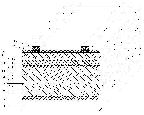
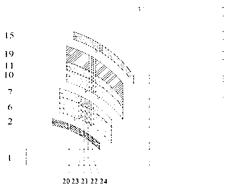
[0051] example 1, figure 2 with diagram 2-1 It is the figure of Embodiment 1 of the present invention
[0052]Using ultra-white glass as the substrate, the copper indium gallium selenide bottom cell is prepared by multi-component co-evaporation three-step method, the cadmium telluride middle cell is prepared by magnetron sputtering method, and the amorphous silicon top cell is prepared by plasma enhanced chemical vapor deposition technology , wherein the first intermediate layer adopts BZO transparent conductive film, and the second intermediate layer adopts silicon oxide low-conductivity transparent film.
[0053] Manufactured as follows:
[0054] Ultra-clear glass is used as the deposition substrate 1 of the three-layer thin-film battery of the present invention. After ultrasonic cleaning and automatic optical detection of defects, DC magnetron sputtering method is used on one side, and by adjusting the pressure of argon gas, the Deposit a layer of high resistance molyb...
example 2
[0079] Ultra-clear glass as the substrate 1, the bottom cell 6 copper indium gallium selenium prepared by multi-component co-evaporation two-step method, the middle cell 10, the cadmium telluride cell was prepared by magnetron sputtering, the amorphous silicon top cell was prepared by plasma enhanced chemistry Manufactured by vapor phase deposition technology, wherein the first intermediate layer is made of silicon oxide low-conductivity transparent film, and the second middle layer is made of AZO transparent conductive film.
[0080] Deposition substrate 1, after ultrasonic cleaning and automatic optical detection of defects, adopts DC magnetron sputtering method on one side, by adjusting the pressure of argon gas, deposits a layer of high resistance molybdenum (Mo) layer under high pressure in sequence, and then Deposit a layer of low-resistance molybdenum (Mo) layer under low pressure, with a total thickness of 1.5 μm, forming the back contact layer 2 of the bottom cell 6; ...
example 3
[0102] Stainless steel is used as the flexible substrate, the copper indium gallium selenide bottom cell 6 is prepared by electrodeposition, the cadmium telluride middle cell 10 is prepared by magnetron sputtering, and the amorphous silicon top cell 19 is prepared by plasma enhanced chemical vapor deposition In the preparation, the first intermediate layer 7 adopts AZO transparent conductive film, and the second intermediate layer 11 adopts silicon oxide low-conductivity transparent film.
[0103] Manufacture takes stainless steel as the substrate 1 of the triple laminated film battery of the present invention, ultrasonically cleans it, adopts DC magnetron sputtering method on its side, and deposits one layer of high-resistance molybdenum (Mo ) layer, and then deposit a layer of low-resistance molybdenum (Mo) layer under low pressure, with a total thickness of 2 μm, forming the back contact layer 2 of the bottom cell;
[0104] The bottom cell is on the back contact layer 2, an...
PUM
| Property | Measurement | Unit |
|---|---|---|
| Thickness | aaaaa | aaaaa |
| Resistivity | aaaaa | aaaaa |
| Thickness | aaaaa | aaaaa |
Abstract
Description
Claims
Application Information
 - R&D
- Intellectual Property
- Life Sciences
- Materials
- Tech Scout
- Unparalleled Data Quality
- Higher Quality Content
- 60% Fewer Hallucinations
Browse by: Latest US Patents, China's latest patents, Technical Efficacy Thesaurus, Application Domain, Technology Topic, Popular Technical Reports.
© 2025 PatSnap. All rights reserved.Legal|Privacy policy|Modern Slavery Act Transparency Statement|Sitemap|About US| Contact US: help@patsnap.com


