Lead-free solder combination and printed circuit board and electronic device provided with lead-free solder combination
A printed circuit board, lead-free solder technology, applied in the direction of welding/cutting medium/material, welding medium, welding equipment, etc., can solve the basic properties of solder, that is, reduce the bonding, improve the influence of slag and discoloration, and melt temperature increase and other problems, to achieve the effect of improving the combination, improving the mechanical properties, and preventing oxidation
- Summary
- Abstract
- Description
- Claims
- Application Information
AI Technical Summary
Problems solved by technology
Method used
Image
Examples
Embodiment approach 1
[0065] This embodiment provides a lead-free solder composition and a PCB and an electronic device using the lead-free solder composition, the composition includes silver from 0.1wt%-4.0wt%, copper from 0.1wt%-2wt%, 0.001wt%-0.05wt% of silicon, 0.001wt%-0.01wt% of cobalt, and the balance of tin.
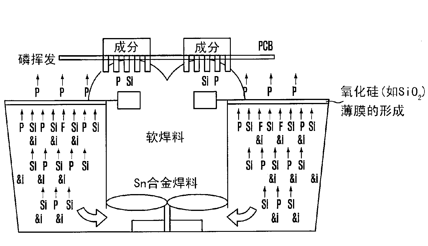
[0066] The following will refer to figure 1 Explain the role of the composition of silicon and cobalt in preventing oxidation.
[0067] figure 1
[0068]
[0069] (Amount of oxidation: the amount of oxide; oxidation rate: oxidation rate; comparative example: comparative example; example: embodiment; after 1 hour: after 1 hour; after 2 hours: after 2 hours; after 3 hours: after 3 hours back.)
[0070] figure 1 Experimental data of the amount of oxides measured by the following method are exemplified. Silicon and cobalt are added to the intended base alloy. The resulting alloy is melted to make a solder composition. The solder composition was heated to 260° C. on a hot plate ...
Embodiment 2
[0318] The high temperature lead-free solder compound according to the present embodiment may include tin (Sn), copper (Cu), silicon (Si), and cobalt (Co).
[0319] The effect of the silicon and cobalt components on the prevention of oxidation will be described below with reference to FIG. 16 .
[0320] Figure 16 illustrates experimental data for the amount of oxides measured by the following procedure. A tin-copper based alloy is prepared and co-melted with either or both silicon and cobalt in a high frequency melting furnace to form a solder compound. After sampling the solder compound, its melting temperature was measured using DSC analysis at 5°C / min. Thereafter, in order to measure the amount of oxide, 3 kg of solder was heated to 420° C. in a SUS crucible having a diameter of 160 mm on a hot plane. Then, the solder compound was stirred at 60 rpm using a stirrer having a diameter of 140 mm for 1 hour, 2 hours, and 3 hours, and oxides were extracted therefrom each time a...
Embodiment 3
[0399] The lead-free solder compound for dilution according to the present embodiment may include nickel (Ni), silicon (Si), phosphorus (P), cobalt (CO), and tin (Sn).
[0400] The effects of the silicon and cobalt components in preventing oxidation will be described below with reference to FIG. 20 .
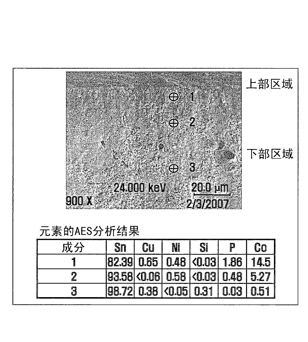
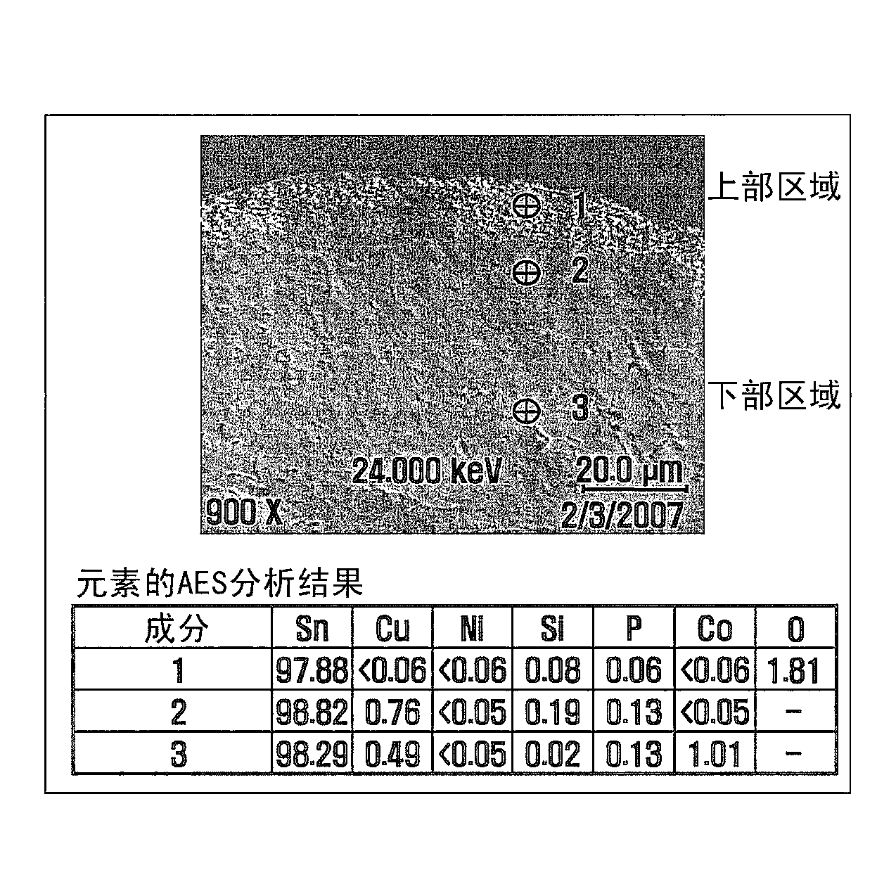
[0401] Figure 20 illustrates experimental data for the amount of oxide measured by the following procedure. Silicon and cobalt are added to Sn-Ni-P based alloys. The resulting alloy is melted to produce a solder compound. On a hot plane, the solder compound was heated to 260°C in a 160mm diameter SUS crucible. Then, the solder compounds were stirred for 1 hour, 2 hours, and 3 hours at a speed of 60 rpm using a stirrer having a diameter of 140 mm, and oxides were extracted therefrom and weighed each time.
[0402] Thereafter, the solder is allowed to solidify, and the solder samples are subsequently cut from the solder. Polish the cut surface of the solder sample. The compos...
PUM
| Property | Measurement | Unit |
|---|---|---|
| melting point | aaaaa | aaaaa |
| melting point | aaaaa | aaaaa |
Abstract
Description
Claims
Application Information
 - R&D Engineer
- R&D Manager
- IP Professional
- Industry Leading Data Capabilities
- Powerful AI technology
- Patent DNA Extraction
Browse by: Latest US Patents, China's latest patents, Technical Efficacy Thesaurus, Application Domain, Technology Topic, Popular Technical Reports.
© 2024 PatSnap. All rights reserved.Legal|Privacy policy|Modern Slavery Act Transparency Statement|Sitemap|About US| Contact US: help@patsnap.com


